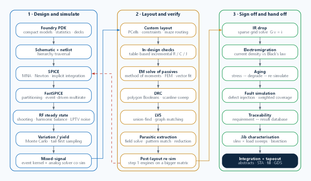
A step-by-step tour of the analog / custom IC design flow — PDK, schematic, SPICE, FastSPICE, RF steady state, Monte Carlo and high-sigma yield, mixed-signal, layout, DRC, LVS, extraction, EM/IR, aging, fault simulation and .lib characterisation — with the purpose of each step and the numerical method inside the tool that answers it.
Posts by alex.novickis@gmail.com
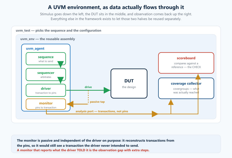
UVM in Practice: The Parts That Earn Their Keep, and the Parts That Do Not
A working engineer’s guide to UVM — the component architecture and why it is shaped that way, the factory and config_db, phasing and objections, sequences and virtual sequences, the register abstraction layer, and an honest account of when UVM is overkill and what to use instead.
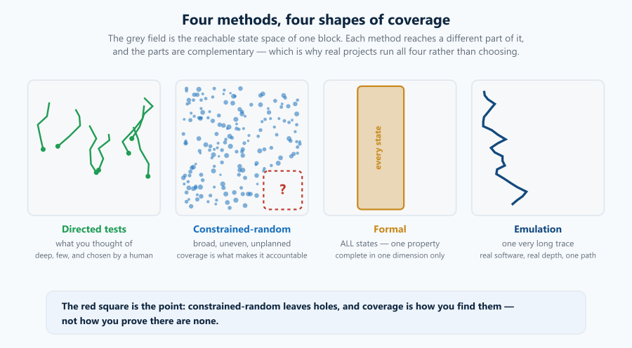
Testbench Methods: What Each One Can Actually Prove
A working guide to hardware verification methods — directed tests, constrained-random, assertions, formal property checking, emulation, software-driven tests and fault injection. What each one proves, what it is structurally blind to, what it costs, and how coverage and checking decide whether any of it means anything.