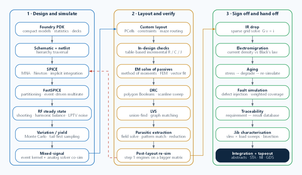
A step-by-step tour of the analog / custom IC design flow — PDK, schematic, SPICE, FastSPICE, RF steady state, Monte Carlo and high-sigma yield, mixed-signal, layout, DRC, LVS, extraction, EM/IR, aging, fault simulation and .lib characterisation — with the purpose of each step and the numerical method inside the tool that answers it. Read More
Category: Circuit Design
UVM in Practice: The Parts That Earn Their Keep, and the Parts That Do Not
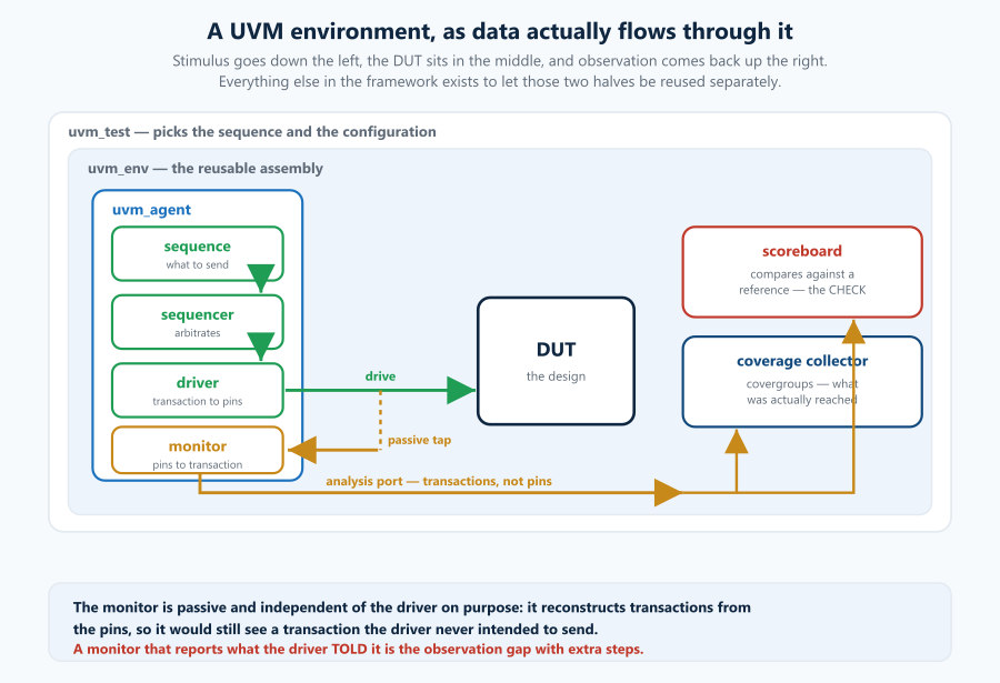
A working engineer’s guide to UVM — the component architecture and why it is shaped that way, the factory and config_db, phasing and objections, sequences and virtual sequences, the register abstraction layer, and an honest account of when UVM is overkill and what to use instead. Read More
Testbench Methods: What Each One Can Actually Prove
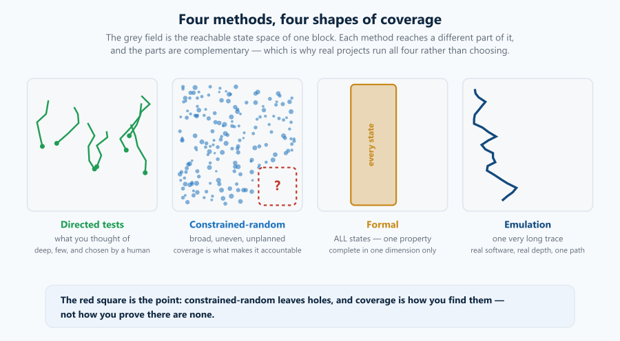
A working guide to hardware verification methods — directed tests, constrained-random, assertions, formal property checking, emulation, software-driven tests and fault injection. What each one proves, what it is structurally blind to, what it costs, and how coverage and checking decide whether any of it means anything. Read More