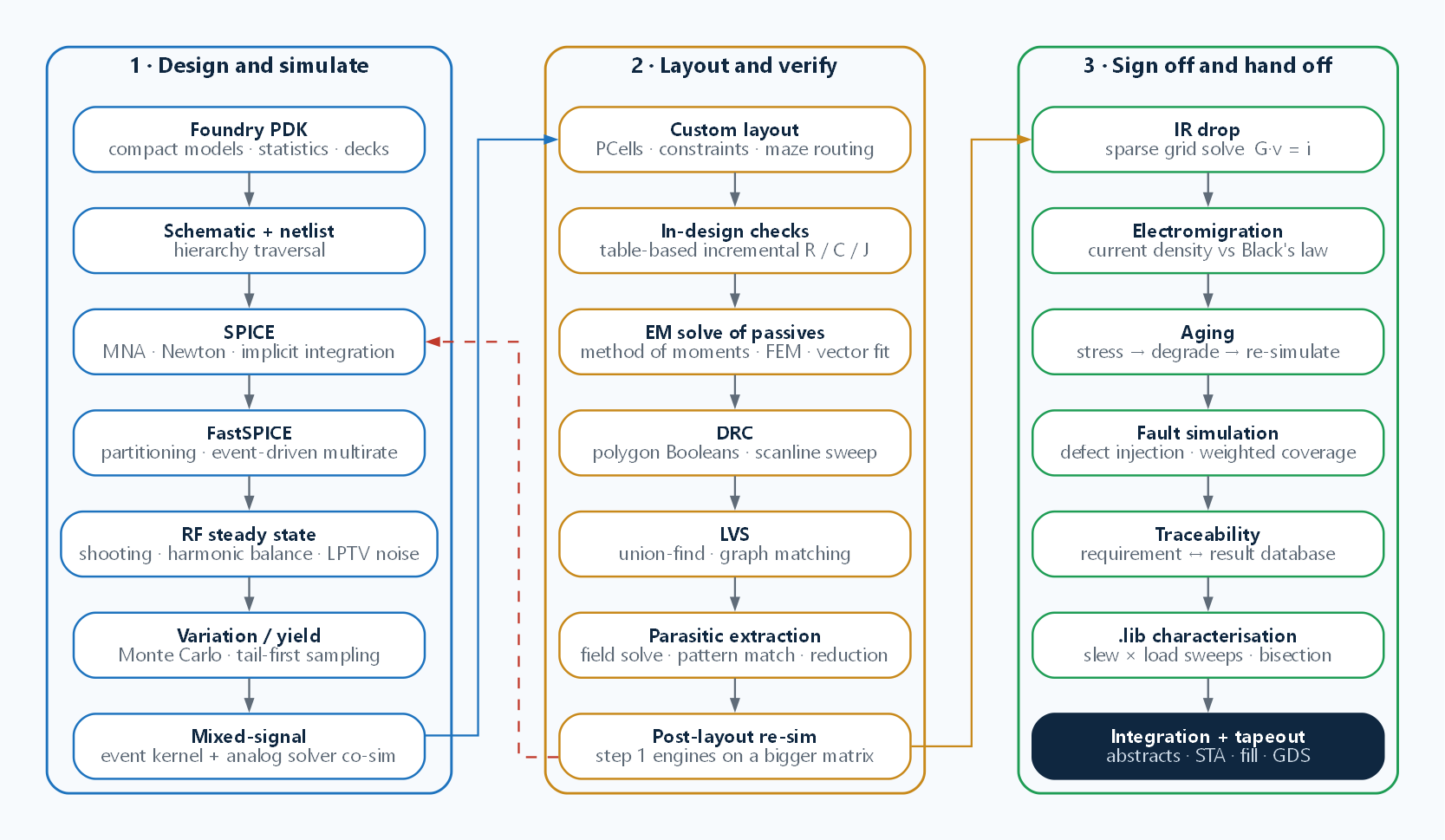
Most write-ups of the analog flow are tool lists: “schematic in Virtuoso, simulate in Spectre, verify in Calibre.” That tells you what to buy, not what is happening. This post is the other half: for every step of the analog / custom IC flow, the question it answers, how the designer drives it, and the numerical method inside the tool that actually produces the answer. If you have ever wondered why a transient run suddenly crawls, why AC analysis says nothing about distortion, or why “zero fails in 200 Monte Carlo runs” is not a yield number, the answers are in the methods.
This is the companion to From Concept to Tapeout: The ASIC Design Flow, Step by Step, which walks the whole chip program and treats analog as one track among many. Here the analog / custom track gets the full treatment. Tool names reference the three vendors that dominate custom IC design: Cadence (Virtuoso, Spectre), Synopsys (Custom Compiler, PrimeSim, StarRC, and the former Ansys signoff tools), and Siemens EDA (Calibre, Solido).
Why the methods matter
Analog design is simulation-driven in a way digital design is not. A digital block is synthesised from RTL, and its correctness is a logic question. An analog block is drawn by hand, and its correctness is a numerical question: does the solution of a few thousand coupled nonlinear differential equations stay inside the spec window at every corner, for every manufactured die, for ten years?
Every tool in the flow is a solver for one piece of that question. Knowing which solver, and what it assumes, is what separates a designer who trusts a green spreadsheet from one who knows when it is lying.
Phase 1 — Design and simulate
1. The foundry PDK
Purpose. The Process Design Kit tells every tool what the process can build and how its devices behave. Every later step is only as correct as the PDK.
How. The foundry ships device models with process corners (TT, FF, SS, FS, SF) and a statistical model, parameterised layout generators (PCells), a technology file, and the rule decks for DRC, LVS, extraction and EM.
The computation. A device model is a compact model — BSIM-CMG for FinFETs, BSIM4 or PSP for planar CMOS. It is a set of closed-form equations: give it the terminal voltages and it returns terminal currents, terminal charges, and their derivatives. The derivatives matter as much as the values, because they become the Jacobian the simulator inverts at every iteration. Model evaluation is often a third to a half of SPICE runtime.
Mismatch between two “identical” transistors follows Pelgrom’s law: the spread shrinks with the square root of gate area.
where is a process constant, typically 1–3 mV·µm. Quadruple the area to halve the mismatch.
That one line is why matched pairs in an analog layout are large, and why the Monte Carlo model in step 6 draws each device’s local parameters from a distribution sized by it.
2. Schematic capture and netlisting
Purpose. The schematic states the circuit: topology, sizes, hierarchy. It is also the reference LVS will later check the layout against.
How. The designer places PDK symbols, sets W, L, fin count and multiplier, and builds hierarchy. A netlister writes the design out as text that a simulator can read.
The computation. Netlisting is a depth-first walk of the hierarchy. At each instance the netlister evaluates parameter expressions, picks which view of each cell to emit (schematic, behavioural model, extracted layout), and names nets by connectivity. The output is a graph: nodes, and device branches between them. That graph is exactly what step 3 turns into equations.
3. SPICE: the reference solver
Cadence Spectre / Spectre X, Synopsys PrimeSim HSPICE / PrimeSim SPICE.
Purpose. Compute node voltages and branch currents with transistor-level accuracy. Every faster method is judged against this.
How. The designer sets up testbenches in an environment (Cadence ADE, Synopsys PrimeWave) and runs DC, AC, noise, transient and stability analyses across corners, then reduces waveforms to numbers: gain, bandwidth, phase margin, settling time.
The computation. Four ideas, stacked.
Modified Nodal Analysis (MNA). Kirchhoff’s current law is written at every node, with the node voltages as unknowns. Voltage sources and inductors add their currents as extra unknowns — the “modified” part. Each device stamps its contribution into a matrix: a resistor between nodes i and j adds +1/R on the two diagonal entries and −1/R on the two off-diagonal ones. The whole circuit becomes one system of differential-algebraic equations:
where x holds the node voltages and branch currents, f the resistive currents, q the charges and fluxes, and u the independent sources.
Newton–Raphson for the nonlinearity. Transistors and diodes are nonlinear, so the system is solved by repeated linearisation:
repeated until both the update and the KCL residual fall below tolerance. When Newton cannot find the DC operating point from a cold start, simulators fall back on homotopy: add a large conductance from every node to ground and shrink it to zero (gmin stepping), or ramp the supplies up from zero (source stepping).
Implicit integration for time. Circuits are stiff: time constants span picoseconds to milliseconds in the same netlist. Explicit methods would need picosecond steps for the whole run. So SPICE uses implicit formulas — backward Euler, trapezoidal, Gear-2 — which turn every time point into a nonlinear algebraic problem, solved by Newton with the Jacobian
where G holds the conductances, C the capacitances, h is the time step, and α depends on the integration formula (α = 1 for backward Euler).
The step size h is chosen by the local truncation error: the simulator compares a cheap extrapolated prediction with the converged answer. A big disagreement means the waveform is moving fast, so h shrinks; a small one lets h grow. This is why the accuracy preset (errpreset in Spectre, accuracy options in HSPICE) changes runtime and answers together.
Sparse LU for the linear solve. Each Newton step solves J·Δx = −r. Circuit matrices are extremely sparse — a handful of non-zeros per row — so sparse LU with a fill-reducing ordering costs far less than the textbook n³. Much of what “Spectre X” or “PrimeSim SPICE” adds is parallel, partitioned factorisation and skipping devices whose voltages did not move.
AC and noise. AC analysis linearises once around the DC operating point and solves a complex linear system per frequency, (G + jωC)·x = u — no Newton, which is why it is fast, and why it knows nothing about distortion or clipping. Noise analysis uses the adjoint trick: one solve of the transposed system per frequency gives the transfer function from every noise source to the output at once. Summing each source’s spectral density through its transfer function produces the noise-summary table that tells you which transistor to fix.
4. FastSPICE: trading a little accuracy for a lot of capacity
Cadence Spectre FX, Synopsys PrimeSim XA / PrimeSim Pro.
Purpose. SPICE does not scale to memories, full-chip analog, or multi-million-device post-layout netlists. FastSPICE gives up roughly 1–5 % on timing and power for 10–1000× speed.
The computation.
- Partition the circuit into channel-connected components — groups of transistors joined source-to-drain, with gates as the boundaries. Each gets its own small matrix.
- Integrate event-driven and multirate. Each partition takes its own time step. A partition whose inputs are quiet is not solved at all. In a big digital-heavy block only a few percent of partitions are active at any instant.
- Simplify the devices. Pre-tabulated I–V and Q–V curves replace full compact-model evaluation.
- Exploit repetition. Identical sub-circuits (bit-cells) are simulated once and shared; parasitic networks are reduced first.
The error lives at partition boundaries, where a strong feedback path is relaxed instead of solved together. That is the rule of thumb in one sentence: FastSPICE is strongest on large, loosely coupled circuits and weakest on tight analog feedback loops. Keep the bandgap and the regulator on SPICE-accurate settings.
5. RF steady state: shooting, harmonic balance, and periodic noise
Cadence Spectre RF, Synopsys PrimeSim HSPICE RF; Keysight ADS for board-plus-chip RF.
Purpose. Mixers, PLLs, oscillators, LNAs and switched-capacitor circuits operate in a periodic large-signal state. Transient would need thousands of cycles to settle and still could not give cyclostationary noise. AC linearises around a DC point that does not exist in operation.
The computation — shooting. Find the starting state x₀ that returns to itself after one period T:
This is solved by Newton on x₀. Each iteration costs about one period of transient, and the sensitivity matrix is never formed explicitly — a matrix-free Krylov solver (GMRES) only needs products with it. A few iterations replace thousands of settling cycles. Shooting is the right tool for strongly nonlinear, sharp-edged circuits: dividers, switched-cap filters, ring oscillators.
The computation — harmonic balance. Write every waveform as a truncated Fourier series and solve for the coefficients directly. Devices cannot be evaluated in the frequency domain, so each iteration inverse-FFTs to time samples, evaluates the transistors there, and FFTs back. Harmonic balance is the better tool for mildly nonlinear, multi-tone circuits — LNAs, power amplifiers, mixers with two-tone intermodulation — and for anything described by S-parameters.
The computation — periodic noise. Linearise around the time-varying steady state instead of a DC point. The result is a periodically time-varying linear system, and noise at each sideband f + k·f₀ folds down to the output frequency:
That folding is how a mixer’s LO harmonics bring noise into the IF band, and it is the basis of oscillator phase-noise analysis. For the RF circuit side of this story see RF and Microwave Design.
6. Variation and high-sigma yield
Cadence Spectre FMC, Siemens Solido Design Environment.
Purpose. Corners check a handful of worst cases. They say nothing about local mismatch and cannot give a yield. When a block is repeated millions of times — an SRAM bit-cell, a comparator in a big ADC array — the per-instance failure rate has to be around one in a billion.
The computation — plain Monte Carlo. Draw random parameter sets, simulate each, count failures. The catch is statistics:
To see a failure probability p with useful confidence you need roughly N ≈ 10/p to 100/p simulations.
At 3σ (p ≈ 1.35 × 10⁻³) that is about ten thousand runs — feasible. At 6σ (p ≈ 10⁻⁹) it is around ten billion — impossible.
The computation — high-sigma methods. Put the simulations where the failures are. Importance sampling draws from a distribution shifted toward the failure region and re-weights each sample by the likelihood ratio. The approach popularised by Solido works differently and is easier to trust: generate a billion candidate samples (just random numbers, so free), simulate a few hundred, fit a surrogate model, use it to sort all candidates by predicted badness, then simulate from the worst end inward until the true tail ordering is confirmed. The 6σ answer is an actual SPICE result at an actual extreme sample, reached with a few thousand simulations instead of a billion.
Worked number. An array of 5 × 10⁸ cells with a 99 % array-yield target and no redundancy needs a per-cell failure probability below about 2 × 10⁻¹¹ — roughly 6.6σ. Brute-force Monte Carlo would need on the order of 10¹² runs. That gap is the entire reason high-sigma tools exist.
7. Mixed-signal verification
Cadence Spectre AMS Designer + Xcelium, Synopsys PrimeSim AMS + VCS.
Purpose. Analog blocks are controlled by digital logic: trim registers, calibration loops, SAR logic, PLL dividers, power sequencing. The worst bugs live at the boundary — a reset polarity, a bit order, a calibration loop that never converges. The analog block has to run inside the real RTL and testbench.
The computation. Two engines run together. The digital kernel is event-driven: time jumps from event to event. The analog solver advances with its own adaptive step. Connect modules sit at every boundary net. Analog-to-digital: the analog engine watches the voltage, finds the threshold-crossing time precisely, and posts a digital event there. Digital-to-analog: an event forces the analog solver to place a time point at that instant, and the connect module drives the net with a defined ramp and output resistance. Throughput is set by how often the two engines have to synchronise.
Real-number models remove the analog solver for the modelled blocks altogether: voltages become real-valued signals that change only at events. That is 10–1000× faster and makes full regression coverage possible — at the price that the model is only as accurate as its author, so the models themselves get checked against SPICE.
Phase 2 — Layout and verify
8. Custom layout
Cadence Virtuoso Layout Suite, Synopsys Custom Compiler.
Purpose. Turn the netlist into the exact polygons the foundry will print. In analog, the layout is part of the design: matching, symmetry, parasitics, coupling and well-proximity effects all move the circuit’s performance.
The computation. PCells are programs: given W, L and finger count, they compute the polygons, so schematic and layout cannot disagree about a device. Connectivity is kept as a live graph linking shapes to schematic nets, which is what flags an open or short while you draw. Automated placement minimises a cost (wire length, area, constraint penalties) by simulated annealing, analytical placement or, in newer tools, learned placement priors. Routing is maze routing or A* search on a track graph, with rip-up-and-reroute for congestion. In multi-patterning nodes, two shapes closer than the single-mask pitch must go on different masks — with two masks that is a check that the conflict graph is bipartite, and an odd cycle is a violation no colouring can fix.
9. In-design electrical checks
Cadence Virtuoso Layout EAD, Synopsys IC Validator Live + in-design StarRC.
Purpose. Shrink the “draw, extract, re-simulate” loop from hours to seconds.
The computation. Incremental extraction from pre-characterised tables — capacitance per unit length versus width, spacing and neighbouring layers, built once by a field solver — recomputed only where the layout changed. Current-density checks import branch currents from a prior simulation and compare each wire segment against the PDK limit:
10. EM solves for inductors, transformers and lines
Cadence EMX and Clarity, Synopsys RaptorX / VeloceRF and HFSS.
Purpose. Spirals, transformers, baluns and on-chip lines have inductance, mutual coupling, skin effect, substrate loss and self-resonance that an RC extractor cannot see. Get them wrong and the VCO lands off frequency.
The computation — method of moments (planar solvers). Only the conductors are meshed; the layered substrate is handled analytically by a Green’s function. The result is a dense matrix equation for the conductor currents, made tractable by FFT- or multipole-style compression. Few unknowns, substrate “for free” — which is why planar solvers are fast for on-chip spirals.
The computation — finite elements (full-wave 3D). The whole volume is meshed with tetrahedra and Maxwell’s equations are solved for the electric field, with adaptive mesh refinement until the S-parameters stop changing. Slower, but it handles bumps, bond wires, packages and connectors — the same solver family we lean on for board-level signal integrity.
Model generation. A table of S-parameters cannot be integrated in time. Vector fitting fits it to a sum of poles and residues, with passivity enforced so the model cannot create energy, and that rational model becomes an equivalent circuit SPICE can simulate.
11. DRC — can it be manufactured?
Siemens Calibre, Cadence Pegasus, Synopsys IC Validator.
Purpose. Prove the layout obeys every manufacturing rule: width, spacing, enclosure, density, antenna ratio, mask colouring. One violation and the foundry rejects the tapeout.
The computation. A rule deck is a program of geometric operations. Layer Booleans derive new layers (a transistor gate is POLY AND DIFF). Edge-pair measurements find edges closer than a limit — width is an internal distance, spacing an external one. The engine underneath is the scanline: sort polygon edges, sweep a line across the layout, keep the active edges in order, and every Boolean or proximity check becomes a local operation on neighbours — about n·log n for n edges. Hierarchical processing checks a cell once and reuses the answer for every placement, which is what makes billion-shape layouts finish overnight.
12. LVS — is it the same circuit?
Purpose. Prove the layout implements the schematic: same devices, same sizes, same connections. Catches shorts, opens, swapped pins and accidental devices.
The computation. Three stages. Device recognition by layer Booleans, with W and L measured off the gate polygon. Connectivity by union-find: every overlap or via merges two sets of shapes into one net, in near-linear time. Comparison of the two netlists as graphs: general graph isomorphism has no known fast algorithm, but circuits suit iterative partition refinement — give every node a signature (device type, pin count, net degree), repeatedly hash each signature with its neighbours’, and the classes split until nodes match uniquely. Labelled ports seed the process; symmetric structures are resolved by trial assignment.
13. Parasitic extraction
Cadence Quantus, Synopsys StarRC, Siemens Calibre xACT.
Purpose. Wires add resistance, capacitance to ground, and coupling to their neighbours — in advanced nodes coupling often dominates. Extraction puts that back into the netlist.
The computation. Capacitance is electrostatics: hold one conductor at 1 V, the rest at 0, solve Laplace’s equation, read off the induced charges. Doing that for every net on a chip is too slow, so production extractors split the job:
- Pattern matching. Once per process, a field solver characterises thousands of canonical cross-sections. At run time the layout is decomposed into those patterns and looked up.
- Random-walk field solvers for the critical nets. They estimate the potential with Monte Carlo walks to conductor surfaces — no mesh, trivially parallel, and they report their own error bar, which makes them the golden reference.
Resistance is computed per segment,
with width- and temperature-dependent corrections to ρ, plus via and contact tables. The raw network can have millions of nodes, so it is reduced: fast nodes are eliminated, and moment-matching (Krylov) methods project the network onto a small model that keeps its low-frequency behaviour and stays passive.
14. Post-layout re-simulation
Purpose. Close the loop: with the wiring included, are the specs still met at every corner? The usual casualties are bandwidth, differential-pair offset from asymmetric parasitics, PLL loop gain, supply ringing and clock coupling.
The computation. Steps 3–6 again, on a much bigger matrix — every RC segment is a node, every coupling capacitor an off-diagonal entry. That growth is why post-layout runs lean on reduction, selective extraction and FastSPICE. A failure here sends you back either to layout (re-route, shield, symmetrise) or to the schematic (re-size, re-think): the dashed loop in the figure at the top.
Phase 3 — Sign off and hand off
15. IR drop and electromigration
Cadence Voltus-XFi, Synopsys Totem-SC / RedHawk-SC and PrimeSim EMIR.
Purpose. Two physical questions. Under worst-case current, how far does each transistor’s supply sag? And will any wire or via wear out within the product’s life — often ten years at 105–125 °C for automotive?
The computation — IR drop. The power grid is a huge resistor network:
where G is the grid conductance matrix (millions to billions of nodes), v the node voltages and i the transistor current draw.
G is symmetric positive-definite and very sparse, so it is solved iteratively — preconditioned conjugate gradient or multigrid — rather than by direct factorisation. Dynamic IR adds decap and package capacitance and time-steps the same way SPICE does.
The computation — electromigration. Wire lifetime follows Black’s equation:
with n ≈ 1–2 and an activation energy E_a ≈ 0.7–0.9 eV for copper.
The PDK turns that into allowed average, RMS and peak current densities per layer, width and temperature, and the tool checks every segment. With n = 2, halving a strap’s width cuts its lifetime by 4× — EM fixes are rarely marginal. The board-level counterpart of this analysis is in Power Integrity: From Static IR Drop to Rapid di/dt.
16. Aging
Cadence Legato / Spectre aging, Synopsys PrimeSim Reliability (MOSRA).
Purpose. Transistors degrade with use — bias-temperature instability and hot-carrier injection raise threshold voltage and lower mobility. A circuit that passes at time zero can drift out of spec after years.
The computation. Two passes. First simulate fresh and record each transistor’s stress (gate and drain voltage, current, temperature over time). Then apply the foundry aging models — typically a power law in time, ΔV_T ∝ tⁿ with n around 0.1–0.25 — to compute each device’s own degradation at end of life, and re-simulate with every device shifted by its own amount. Because each transistor sees different stress, aging can create mismatch in a pair that was perfectly matched when new.
17. Analog fault simulation
Synopsys PrimeSim Custom Fault, Siemens Tessent DefectSim, Cadence Legato.
Purpose. Two related questions. For production test: if a manufacturing defect occurs, does the test catch it? For functional safety under ISO 26262: if a random hardware fault occurs in the field, does a safety mechanism detect it? The second answer feeds the FMEDA and its metrics.
The computation. Build a defect universe — opens and shorts at device terminals, resistive bridges, parametric shifts (IEEE P2427 standardises how). For each defect: inject it, simulate the test or diagnostic stimulus, compare against the fault-free response, and classify it as detected or not. Coverage is weighted by likelihood, because a short between two wide, closely spaced lines is far likelier than one between distant ones; the weight comes from layout critical area.
where w_d is the likelihood weight of defect d.
Thousands of full simulations per block are normal, so campaigns collapse equivalent faults, stop each run as soon as the fault is detected, and sample statistically with a confidence interval when the universe is too big.
This is the step where the analog flow meets the safety case, and where most of the arguments with assessors happen: what counts as “detected”, which tolerance band, which defects were collapsed away, and whether the coverage number that reaches the FMEDA is the one the simulation actually produced.
18. Requirements traceability
Purpose. Safety and quality standards want evidence that every requirement was verified, by which test, with what result, on which design version.
The computation. Bookkeeping, not numerics — a database linking requirement, testbench, spec, result and design version, rolling coverage up the requirement tree and flagging results produced on a stale version. Cadence’s ADE Verifier does this inside the analog environment.
19. Timing models for the digital side
Cadence Liberate AMS, Synopsys PrimeLib.
Purpose. Static timing analysis cannot simulate transistors; it needs a Liberty (.lib) model of the macro’s digital pins — pin capacitance, clock-to-output delay, setup and hold.
The computation. For each timing arc, a SPICE transient at every point of an input-slew × output-load grid fills a lookup table that STA interpolates. Setup and hold have no direct measurement: the tool bisects on the data-to-clock offset to find where clock-to-output delay degrades by a set percentage, so each point costs about log₂(range ⁄ resolution) simulations. The model must match the SoC’s STA engine, or the integration team chases phantom violations.
20. Integration and tapeout
Purpose. Drop the macro into the SoC and hand clean mask data to the foundry.
The computation. Generate an abstract (pin locations, blockages, antenna data), place it, run STA with the .lib from step 19, insert metal fill so every density window lands between its minimum and maximum (timing-aware fill keeps dummy metal off critical nets), and re-run DRC and LVS on the full chip with the same algorithms as steps 11–12 — now across hundreds of cores. Then stream out GDSII or OASIS.
The same flow in vendor tools
The methods above are vendor-neutral; the tools are not. Below is the same flow drawn three ways: an all-Cadence flow, an all-Synopsys flow, and a best-of-class mix. Diamonds are decisions, and the red return paths are the loops that dominate a real schedule:
- Specs not met pre-layout goes back to the schematic.
- DRC / LVS not clean goes back to layout.
- Specs not met post-layout goes back to layout or to the circuit.
Click a heading to expand its chart.
Cadence analog / custom flow
Synopsys analog / custom flow
Best-of-class mixed flow
Stage-by-stage equivalents.
| Stage | Cadence | Synopsys |
|---|---|---|
| Schematic + layout | Virtuoso Studio | Custom Compiler |
| Simulation environment | ADE Explorer / Assembler | PrimeWave |
| SPICE | Spectre / Spectre X | PrimeSim HSPICE / PrimeSim SPICE |
| FastSPICE | Spectre FX | PrimeSim XA / Pro |
| RF steady state | Spectre RF | PrimeSim HSPICE RF |
| Mixed-signal | Spectre AMS Designer + Xcelium | PrimeSim AMS + VCS |
| In-design checks | Virtuoso Layout EAD | IC Validator Live + in-design StarRC |
| On-chip passives | EMX / Clarity | RaptorX / VeloceRF / HFSS |
| DRC / LVS | Pegasus | IC Validator |
| Extraction | Quantus | StarRC |
| EM / IR | Voltus-XFi / Spectre EMIR | PrimeSim EMIR / RedHawk-SC / Totem-SC |
| Aging | Legato / Spectre aging | PrimeSim Reliability (MOSRA) |
| Analog fault simulation | Legato | PrimeSim Custom Fault |
| .lib characterisation | Liberate AMS | PrimeLib |
The rule behind the mixed flow has three parts:
- Design productivity: use whatever your designers are fastest in.
- Signoff: use whatever the foundry treats as golden. That is usually Calibre for DRC/LVS, and a foundry-qualified extractor.
- Anything facing the digital team: match their simulator and their STA engine, or the integration chases phantom differences.
Mixing has a cost. When two tools disagree, each vendor points at the other. So a mixed flow needs its own correlation habit, repeated once per PDK version:
- run a reference circuit through both SPICE engines;
- compare the two extractors on a few critical nets.
What each tool actually does
Product pages describe these tools in terms of benefits. This section describes them in terms of work: what you feed each tool, what it gives back, what you actually do with it, and where it runs out of road. Tools are grouped by the job they do, with Cadence, Synopsys, Siemens and Keysight options side by side.
Design environment: schematic, layout, and the simulation cockpit
Virtuoso Schematic Editor (Cadence)
- In: PDK symbols and device parameters. Out: an OpenAccess schematic, netlisted to Spectre, HSPICE or CDL.
- What you do with it: draw the transistor-level circuit, set W / L / fingers / multiplier through the CDF forms, and build hierarchy. The XL tier adds a constraint manager: you tag matched pairs, symmetry axes and net classes, and those constraints travel into layout.
- Scripting: everything is reachable from SKILL, which is how teams automate netlisting, checks and bulk edits.
ADE Explorer / ADE Assembler / ADE Verifier (Cadence)
- Explorer is one testbench at a time. You set analyses, sweep a variable, add corners, and write measurement expressions in the waveform calculator.
- Assembler is many testbenches at once. It runs the corner × sweep × Monte Carlo matrix on a farm and shows one pass / fail spec sheet across all of it. That spec sheet is where most analog sign-off evidence actually lives.
- Verifier links requirements to Assembler results, so you can show which requirement is covered by which test, and whether that result is current.
- Scripting: OCEAN (SKILL-based) runs the same setups in batch.
Virtuoso Layout Suite L / XL / EXL (Cadence)
- L is a polygon editor: draw shapes, place PCells, run DRC.
- XL is connectivity-driven. It generates devices from the schematic, shows unrouted connections as flight lines, flags shorts and opens as you draw, and enforces the schematic’s constraints.
- EXL adds automation: analog placement, device-array generation (common-centroid, interdigitated), and routing assistance.
- Watch out: automation gets you a legal starting point. Matching-critical structures are still usually finished by hand.
Virtuoso Layout EAD (Cadence)
- In: a layout in progress, plus currents from a prior simulation.
- Out: live per-net R and C estimates, and current-density violations, while you draw.
- What you do with it: catch a wire that is too thin for its current, or a differential pair with unequal parasitics, before running full extraction.
- Watch out: the numbers are table-based estimates for steering, not signoff values.
Custom Compiler (Synopsys)
- In: PDK and schematic. Out: OpenAccess schematic and layout.
- What you do with it: the same jobs as Virtuoso schematic plus layout: template- and constraint-driven layout assistance, in-design DRC through IC Validator Live, and in-design parasitics through StarRC.
- Watch out: it can open IC Compiler II databases directly, which matters when analog and digital share a floorplan. Check that your foundry ships the PDK for Custom Compiler, not only for Virtuoso.
PrimeWave (Synopsys)
- Custom Compiler’s simulation cockpit, and the counterpart of ADE: testbench setup, corners, Monte Carlo, spec tables, and waveform viewing for the PrimeSim engines.
Circuit simulators
Spectre / Spectre X (Cadence)
- In: netlist plus PDK models. Out: waveforms, operating points, noise summaries.
- Analyses: DC, AC, noise, transient, stability (stb), pole-zero, sensitivity.
- Spectre X is the same engine with multithreading and distributed runs, and accuracy chosen with one preset (+preset=cx through vx).
- What you do with it: everything that needs transistor-level accuracy on a block up to roughly hundreds of thousands of devices.
Spectre FX (Cadence)
- FastSPICE: the partitioned, event-driven engine from step 4, for full-chip analog, memory, and large post-layout netlists.
- What you do with it: check connectivity, power-up sequencing and functional behaviour at a scale where Spectre X would take days.
- Watch out: keep references, regulators and tight feedback loops on SPICE-accurate settings.
Spectre RF option (Cadence)
- Analyses: PSS / HB periodic steady state; PAC, PXF and PSTB small-signal around it; Pnoise (including phase and jitter); QPSS for multi-tone; envelope for modulated signals.
- What you do with it: mixer conversion gain and noise figure, VCO phase noise, PLL jitter contributions, LNA compression and IP3, switched-capacitor filter response.
Spectre FMC (Cadence)
- Fast Monte Carlo: picks the samples most likely to fail so it can estimate 3–6σ yield with far fewer runs than brute force. It runs inside ADE Assembler.
Spectre aging / reliability (Cadence)
- In: a mission profile (lifetime, temperature, supply). Out: fresh-vs-aged results per spec, from the stress → degrade → re-simulate method in step 16.
PrimeSim HSPICE (Synopsys)
- The long-standing reference simulator, and many foundries validate their models against it first.
- Features engineers lean on:.measure for scripted measurements, .alter for netlist variants, built-in Monte Carlo, RF harmonic balance, and signal-integrity features (W-element transmission lines, statistical eye analysis).
- What you do with it: golden cross-checks, model correlation, and characterisation decks.
PrimeSim SPICE / PrimeSim XA / PrimeSim Pro (Synopsys)
- PrimeSim SPICE is the accelerated SPICE engine, using multicore and GPU.
- XA is FastSPICE for mixed-signal and custom digital blocks.
- Pro targets very large netlists, such as DRAM / flash arrays and big post-layout runs.
- Same division of labour as Spectre X / FX.
Keysight ADS (Keysight)
- RF and microwave circuit simulation (harmonic balance, circuit envelope, transient with S-parameter blocks), plus the Momentum planar and FEM EM solvers in the same environment.
- What you do with it: RF front-ends, matching networks, and module- and board-level RF, where the circuit meets the package and the PCB.
- Watch out: RFIC teams on Virtuoso usually keep the chip in Spectre RF and use ADS for the off-chip parts.
Variation and yield
Solido Design Environment (Siemens)
- Drives Spectre or HSPICE from inside ADE to run variation-aware analyses: PVT corner reduction, Monte Carlo, and high-sigma verification.
- High-sigma uses the “simulate the tail first” ordering from step 6, so a 6σ answer comes from a few thousand real SPICE runs.
- What you do with it: bit-cell and sense-amp yield, comparator offset at array scale, and finding the few corners that actually matter out of hundreds.
Mixed-signal verification
Spectre AMS Designer + Xcelium (Cadence) and PrimeSim AMS + VCS (Synopsys)
- In: SystemVerilog / UVM testbench and RTL, plus analog blocks as SPICE netlists, Verilog-AMS models, or real-number models.
- Out: one co-simulation, with connect modules inserted automatically at every analog–digital boundary.
- What you do with it: run the digital team’s regression with real analog behaviour in the loop, such as trim and calibration loops, reset and power sequencing, and ADC / DAC interfaces.
- Which to pick: use whichever simulator the digital team already uses. Xcelium and VCS are also the standalone digital simulators.
Physical verification and extraction
Calibre nmDRC / nmLVS (Siemens)
- In: GDS / OASIS or OpenAccess layout, the source netlist, and the foundry rule deck. Out: a violation database, browsed in Calibre RVE with cross-probing into the layout editor.
- What you do with it: foundry signoff DRC and LVS. Calibre runsets are usually the first ones a foundry qualifies.
- Calibre RealTime Custom runs the same deck incrementally inside Virtuoso or Custom Compiler as you draw.
- Calibre PERC checks reliability rules that pure geometry can’t express, such as ESD paths and voltage-dependent spacing.
Pegasus (Cadence) and IC Validator (Synopsys)
- The same DRC / LVS job, with each vendor’s own engine built to scale across many CPUs.
- Both have in-design modes: iPegasus in Virtuoso, and IC Validator Live in Custom Compiler.
- Use either for signoff when the foundry ships and qualifies its deck.
Quantus (Cadence), StarRC (Synopsys), Calibre xACT (Siemens)
- In: layout plus the foundry extraction techfile. Out: an RC or RLC netlist (DSPF / SPEF) or an extracted view that the simulator reads directly.
- What you do with it: decide the extraction mode per net — C-only, RC, or coupled — and the reduction level. Run the field-solver mode on the handful of nets where accuracy matters.
- StarRC is also the extractor behind PrimeTime, which keeps analog and digital parasitics consistent at a block boundary.
EM solvers for passives and packages
EMX (Cadence)
- In: inductor, transformer or line geometry plus the process stack-up. Out: S-parameters and fitted SPICE models.
- A planar method-of-moments solver, fast enough to run inside the design loop.
RaptorX / VeloceRF (Synopsys)
- RaptorX does the same job as EMX, and also extracts EM coupling across larger layout regions.
- VeloceRF synthesises inductors and transformers. You give it target L, Q and frequency, and it returns the geometry.
HFSS (Synopsys, formerly Ansys) and Clarity 3D Solver (Cadence)
- Full-wave 3D FEM for packages, bumps, bond wires, connectors and anything else that is genuinely three-dimensional.
- In: 3D geometry and materials. Out: broadband S-parameters.
- Slower than planar solvers, but they make no layered-substrate assumption.
Power, reliability and safety signoff
Voltus-XFi / Spectre EMIR (Cadence) and PrimeSim EMIR (Synopsys)
- Transistor-level IR-drop and electromigration analysis, using currents from a real Spectre or PrimeSim run on the extracted netlist.
- What you do with it: find the strap, via or finger that violates its current-density limit, and the transistors whose supply sags too far under worst-case load.
Totem-SC / RedHawk-SC (Synopsys, formerly Ansys)
- Totem-SC is transistor-level EM/IR for analog and custom blocks.
- RedHawk-SC is the SoC-level dynamic power, IR and EM tool.
- What you do with them: foundry-certified power-integrity signoff. In a mixed-signal chip the analog macro’s model is handed to the SoC-level run.
Legato Reliability (Cadence)
- Reliability analysis around Spectre: device aging, electromigration and thermal effects, plus analog defect simulation.
PrimeSim Reliability (MOSRA) (Synopsys)
- Aging with foundry BTI / HCI models in the PrimeSim / HSPICE flow.
PrimeSim Custom Fault (Synopsys) and Tessent DefectSim (Siemens)
- In: the netlist, a defect model (opens, shorts, bridges, parametric shifts), the test or diagnostic stimulus, and a detection criterion.
- Out: per-defect detected / undetected results and likelihood-weighted coverage.
- What you do with it: prove production-test coverage, and produce the analog diagnostic-coverage numbers an ISO 26262 FMEDA needs.
Hand-off to the digital side
Liberate AMS (Cadence) and PrimeLib (Synopsys)
- In: the macro’s netlist, its pin and arc definitions, and the slew / load index tables. Out: a Liberty (.lib) model with timing, power and pin capacitance (NLDM / CCS).
- What you do with it: give STA a correct view of the macro’s digital interface.
- Which to pick: use the one matching the SoC’s STA engine — Liberate for Tempus, PrimeLib for PrimeTime.
Innovus (Cadence) and Fusion Compiler / IC Compiler II (Synopsys)
- Digital place-and-route.
- For the analog block, they: place the macro from its abstract (LEF), route power to it, respect its keep-out halo, and close timing on the interface. Nothing inside the macro is touched.
Five things the methods explain
- Why loose accuracy presets are dangerous. The truncation-error step control is what keeps a transient honest. Loosen it and settling times, FFT noise floors and oscillation onset all move — with no warning.
- Why AC loop gain can lie. AC linearises around a DC point. A switched or large-signal loop has no meaningful DC point; use periodic stability analysis on the steady state.
- Why FastSPICE and bandgaps do not mix. Partitioning relaxes exactly the tight feedback a reference or regulator depends on.
- Why “0 fails in 200 runs” is not a yield. With N = 200 the 95 % upper bound on the failure rate is still about 1.5 % — roughly 2σ. Report the confidence interval, or use a high-sigma method.
- Why EM and aging need real stimulus. Both are driven by per-device currents and stresses. Vectorless estimates and DC-only aging miss the asymmetries that actually fail.
Further reading
Simulation algorithms
- Kenneth S. Kundert, The Designer’s Guide to SPICE and Spectre.
- Kundert, White & Sangiovanni-Vincentelli, Steady-State Methods for Simulating Analog and Microwave Circuits.
- Vlach & Singhal, Computer Methods for Circuit Analysis and Design.
Layout and variation
- Alan Hastings, The Art of Analog Layout.
- M. Pelgrom et al., “Matching properties of MOS transistors,” IEEE JSSC, 1989 (doi:10.1109/JSSC.1989.572629).
Extraction, EM and reliability
- Odabasioglu, Celik & Pileggi, “PRIMA: passive reduced-order interconnect macromodeling,” IEEE TCAD, 1998 (doi:10.1109/43.712097).
- Gustavsen & Semlyen, “Rational approximation of frequency domain responses by vector fitting,” IEEE Trans. Power Delivery, 1999 (doi:10.1109/61.772353).
- J. R. Black, “Electromigration — a brief survey and some recent results,” IEEE Trans. Electron Devices, 1969 (doi:10.1109/T-ED.1969.16754).
Functional safety
- ISO 26262:2018, Road vehicles — Functional safety (Parts 5 and 11 for hardware and semiconductors).
The step where these methods most often turn into an argument is fault simulation feeding an FMEDA — what was injected, what counted as detected, and whether the coverage in the safety case is the coverage the simulation produced. Reviewing that chain, at chip and board level, is what we do. Reach us at circuit-design.space.
circuit-design.space · +1-971-357-1400 · anovickis@circuit-design.space