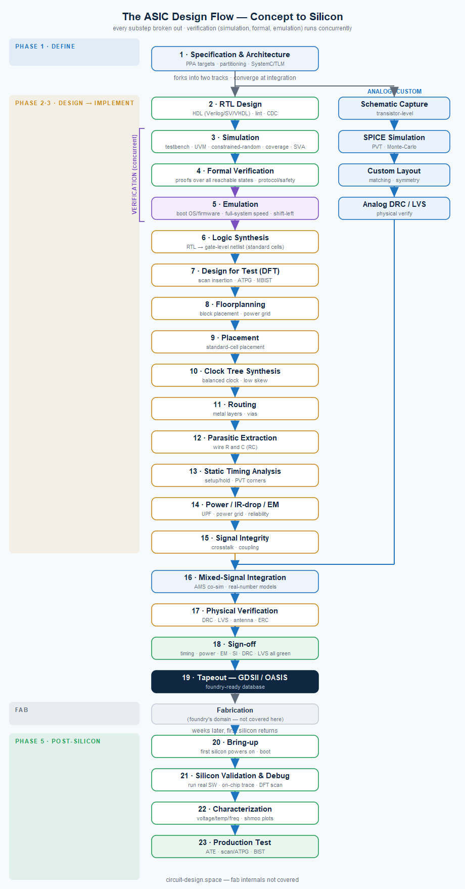
One of the questions I get most often: “what actually happens between an idea for a chip and a design that’s ready to manufacture?” This is that walkthrough — the engineering end of the flow, concept to tapeout, with every step broken out: why it exists, what it produces, how it does it, roughly how long it takes, and the industry-standard tools used. It stops where the design leaves engineering and goes to the foundry; what happens inside the fab is a separate story.
An ASIC (Application-Specific Integrated Circuit) is a chip built for one job, as opposed to a general-purpose part you program after the fact. Designing one is a long pipeline of specialized steps, and the flow forks into two tracks that run in parallel and converge at the end: a digital track that is highly automated and synthesis-driven, and an analog / custom track that is hand-crafted and simulation-driven. Most real chips are mixed-signal — they need both.
Below, each step lists why it exists, its goal, how it works, a typical duration, and the tools — referencing the four vendors that dominate production EDA (electronic design automation): Synopsys, Cadence, Siemens EDA (formerly Mentor Graphics), and Ansys.
How to read the step tags. Each step is marked serial (it can’t start until the previous one finishes — its input is the previous step’s output) or concurrent (it overlaps with its neighbors, run at the same time on the same design). The durations are rough figures for a moderately complex SoC and vary enormously with size, node, and team; a run of one tool takes hours, but the activity around it iterates for weeks. End to end, a complex chip is typically a 1–3 year program. A separate ISO 26262 ASIL B/D safety overlay — for chips that go into cars — runs alongside the whole flow; it’s covered at the end.
Phase 1 — Define
1. Specification and architecture
Serial · typically 1–6 months.
Why. Everything downstream is built against this. A wrong architectural choice — too little memory bandwidth, the wrong bus, an unrealistic clock target — is essentially free to fix here and catastrophically expensive to fix after tapeout. This is the highest-leverage step in the whole flow.
Goal. A specification precise enough to design against, and an architecture that will hit the PPA (power, performance, area) targets.
How. Architects turn a product idea into a concrete engineering spec: what the chip must do, its interfaces, its PPA budget, and how the work is partitioned into blocks. They explore trade-offs — how many cores, how much cache, which memory and I/O standards — usually against an executable model of the system (SystemC/TLM transaction-level models) so performance and power can be profiled before any RTL exists.
Tools. Architectural and virtual-platform modeling — Synopsys Platform Architect and Cadence system design and verification.
Phase 2 — Design and verify (the “front end”)
2. RTL design
Serial (starts the front end) · typically 2–9 months, overlapping verification.
Why. This is the human-authored heart of the chip. Every later step is a mechanical (or verified) transformation of this description; if the RTL is wrong, the silicon is wrong.
Goal. Synthesizable, lint-clean RTL that correctly implements the architecture.
How. Engineers describe the chip’s behavior in a hardware description language (HDL) — Verilog, SystemVerilog, or VHDL — at the register-transfer level (RTL), specifying what happens to data as it moves between registers on each clock edge. Static checks run continuously as they write: lint (style and bug patterns) and CDC (clock-domain-crossing analysis, which catches metastability hazards where signals pass between unrelated clocks).
Tools. Lint and CDC — Synopsys VC SpyGlass, Cadence, and Siemens EDA Questa.
Verification runs concurrently. The next three steps — simulation, formal, and emulation — are not sequential stages. They run in parallel with each other and overlap RTL design: as each block stabilizes, all three engines attack it at once, each answering a question the others can’t. Together they are usually the single largest effort in the whole project.
3. Simulation
Concurrent (with steps 2, 4, 5) · continuous through the front end; often 40–60% of project effort.
Why. Simulation is the workhorse that proves the RTL does what the spec says — and, just as important, does not do what it shouldn’t. A functional bug that escapes here becomes a silicon respin: months and millions.
Goal. High functional coverage — quantified evidence that the intended behaviors have actually been exercised — with zero failing checks.
How. The RTL runs against a testbench, usually built in UVM (the Universal Verification Methodology, a standardized SystemVerilog framework of drivers, monitors, scoreboards, and coverage). Modern DV is constrained-random: instead of hand-writing every case, the testbench generates randomized-but-legal stimulus and tracks coverage to see which scenarios have been hit. SVA (SystemVerilog Assertions) embed checks directly in the design so violations are caught the instant they happen.
Tools.Synopsys VCS, Cadence Xcelium, Siemens EDA Questa.
4. Formal verification
Concurrent (with steps 2, 3, 5) · days to weeks per property set.
Why. Simulation samples behavior with stimulus; it can only ever hit the cases you generate. Formal proves properties mathematically over all reachable states — so it catches corner cases no directed test would think to try. It’s the right tool for control logic, protocol correctness, and safety mechanisms.
Goal. Mathematically proven properties (or a concrete counter-example waveform when one fails), covering behaviors exhaustively rather than by sampling.
How. Properties are written as assertions and handed to a formal engine, which uses techniques like bounded model checking and k-induction to prove them over the design’s entire reachable state space, or produce the shortest trace that violates them.
Tools.Synopsys VC Formal and Cadence JasperGold.
5. Emulation and prototyping
Concurrent (with steps 2–4), begins once RTL is stable · brings up over weeks, then runs for months.
Why. A large SoC simulates at a handful of cycles per second — far too slow to boot an operating system or run real software. Emulation maps the RTL onto special-purpose hardware so it runs millions of times faster, which is the only practical way to exercise the whole system and to give firmware teams a target before silicon exists (the shift-left bridge, so software is ready on day one of bring-up).
Goal. Prove the assembled system runs — boots an OS/RTOS, executes driver and firmware stacks, survives long soak tests and real traffic — and get software validated pre-silicon.
How. The RTL is compiled onto an emulator (a large array of FPGAs or custom processors) or an FPGA prototype, then driven with real software and real interface traffic at near-hardware speed.
Tools.Synopsys ZeBu, Cadence Palladium, and Siemens EDA Veloce.
In short: simulation and formal prove the blocks are right; emulation proves the assembled system runs.
Where pre-verified IP saves you. Every block you buy already-verified is front-end effort you don’t repeat. Our safety soft-IP catalog ships each block with its FMEDA and a self-checking testbench, and our Verification IP provides independent, clean-room checkers to verify your own RTL against a genuine second source.
Phase 3 — Implement (the “back end” / physical design)
6. Logic synthesis
Serial · a run is hours to a day; the activity iterates over weeks.
Why. RTL describes behavior; a foundry builds gates. Synthesis is the bridge — and it’s where the first hard PPA optimization happens, because the same RTL can map to very different gate structures depending on the constraints.
Goal. A gate-level netlist that is logically equivalent to the RTL and meets the PPA targets.
How. The tool translates RTL into an interconnection of standard cells (pre- characterized gates and flip-flops from the foundry’s library), optimizing timing, area, and power against a formal timing-constraint file (SDC). Equivalence checking then proves the netlist still matches the RTL.
Tools.Synopsys Design Compiler and Fusion Compiler; Cadence Genus.
7. Design for test (DFT)
Serial (inserted around synthesis) · typically 2–6 weeks.
Why. Fabrication is imperfect — some dies come out defective. Without on-chip test structures there’s no economical way to tell a good die from a bad one, and defects ship to customers.
Goal. High test coverage so defective dies are caught and discarded after fabrication, protecting the quality of shipped parts.
How. The tool stitches flip-flops into scan chains (shift registers that load and observe test patterns), runs ATPG (Automatic Test Pattern Generation) to compute the patterns that expose faults, and inserts BIST/MBIST (built-in self-test, especially for embedded memories).
Tools.Synopsys TestMAX, Cadence Modus, and Siemens EDA Tessent.
Physical implementation is strictly serial. The next four steps — floorplanning, placement, clock tree synthesis, routing — happen in order, each consuming the previous step’s result, and (importantly) they run inside the same place-and-route tool. You don’t route before you’ve placed; you don’t place before you’ve floorplanned. They’re listed separately because each is a distinct optimization problem with its own goal — but they are one continuous, ordered database being refined, not four independent tools.
8. Floorplanning
Serial (P&R step 1 of 4) · days to ~3 weeks, highly iterative early on.
Why. The floorplan sets the stage for everything physical: get the big blocks or the power grid wrong and no amount of clever placement or routing later can recover the timing or the power delivery.
Goal. A chip-level arrangement in which every block fits, the aspect ratio and pin locations are sane, and power can be delivered cleanly.
How. The engineer decides where the major blocks, memories, and I/O sit, defines the power grid (the mesh of power/ground rails), and reserves routing and placement resources. This is the most human-guided of the physical steps.
Tools.Synopsys Fusion Compiler / IC Compiler II and Cadence Innovus — the same tool used for steps 9–11.
9. Placement
Serial (P&R step 2 of 4) · a run is hours to a day; iterate over days–weeks.
Why. Where each cell sits determines how long its wires are, and wire length dominates delay and power at modern nodes. Placement quality sets the ceiling on the timing the design can ultimately close at.
Goal. A legal, timing-aware placement of every standard cell that leaves the design routable.
How. The tool positions hundreds of thousands to billions of standard cells to minimize wire length and timing cost while obeying density and congestion limits, running incremental timing optimization as it goes.
Tools. Same place-and-route tool as step 8 — Synopsys Fusion Compiler / IC Compiler II, Cadence Innovus.
10. Clock tree synthesis (CTS)
Serial (P&R step 3 of 4) · hours to a couple of days per run.
Why. Every flip-flop needs the clock to arrive at nearly the same instant. Uncontrolled clock arrival (skew) directly eats into the timing budget and can break the chip outright.
Goal. A balanced clock-distribution network that reaches every flip-flop with minimal skew and acceptable insertion delay and power.
How. The tool builds a physical tree (or mesh) of buffers and inverters that distributes the clock, balancing path delays to equalize arrival times, then re-optimizes timing around the now-real clock.
Tools. Same place-and-route tool as steps 8–9.
11. Routing
Serial (P&R step 4 of 4) · one to several days per run; iterate over weeks.
Why. This is where the design becomes physically complete — every logical connection becomes actual metal. It’s also where late timing, signal-integrity, and manufacturability problems concentrate.
Goal. Every net connected in real metal, with no design-rule violations and timing still met.
How. The router connects all cells with wires across the chip’s many metal layers, inserting vias between layers, honoring spacing/width rules and the timing and signal-integrity constraints, and repairing violations iteratively.
Tools. Same place-and-route tool as steps 8–10.
Post-route analysis and sign-off is an iterative loop. The next steps — extraction, timing, power, and signal integrity — all read the routed layout, and a fix demanded by one (say, a timing repair) changes the inputs to the others, so the design loops through them repeatedly until everything closes at once.
12. Parasitic extraction
Serial input to sign-off (loops with 13–15) · hours per run.
Why. At modern nodes the wires themselves — their resistance and capacitance — dominate delay and power. Signing off on estimated wire models would be signing off on a fiction.
Goal. Accurate electrical (RC) models of the physical interconnect, so every downstream sign-off reflects the real layout.
How. The extractor measures the resistance and capacitance of every routed wire and via from the layout geometry and the process stack, producing an annotated model (SPEF) that feeds timing, power, and SI analysis.
Tools.Synopsys StarRC and Cadence Quantus.
13. Static timing analysis (STA)
Iterative sign-off (loops with 12, 14, 15) · a run is hours; iterate across the whole back end.
Why. The chip must run at its target frequency not just nominally, but at the slow-cold and fast-hot extremes of manufacturing and use. Checking that by simulation would be hopeless; STA does it exhaustively without simulation.
Goal.Timing closure — every path proven to meet setup and hold across all conditions.
How. STA walks every signal path and checks its setup/hold margins over multiple PVT corners (process, voltage, temperature) and operating modes, using the extracted parasitics for accuracy. Failing paths are fed back to placement/routing/CTS for repair.
Tools.Synopsys PrimeTime — the long-standing sign-off standard — and Cadence Tempus.
14. Power, IR-drop and electromigration
Iterative sign-off (loops with 12, 13, 15) · hours to days per run.
Why. A chip that meets timing can still fail if it can’t be powered correctly — the grid sags, the metal erodes, or it overheats. These are lifetime-reliability and correctness issues, not nice-to-haves.
Goal. A power-delivery network and thermal profile that keep every transistor inside its safe operating envelope for the life of the product.
How.Power analysis covers dynamic, static, and leakage power; IR-drop analysis checks the grid voltage doesn’t sag too far under load; electromigration (EM) checks current density won’t erode the metal over time; thermal analysis checks temperature. Power intent is captured formally in a UPF (Unified Power Format) file describing domains, switching, and isolation.
Tools.Ansys RedHawk-SC for power integrity, IR-drop, and EM; Cadence Voltus; Ansys Totem for the analog side.
15. Signal integrity (SI)
Iterative sign-off (loops with 12–14) · hours per run.
Why. Densely packed wires switching fast couple into each other. Uncontrolled crosstalk adds delay or injects glitches, silently breaking a design that “passed” nominal timing.
Goal. Signals that arrive clean and on time despite dense, coupled interconnect.
How. SI analysis quantifies crosstalk-induced delay and noise and feeds the effect back into timing; on high-speed I/O it extends to full electromagnetic channel modeling.
Tools. Analyzed within the timing/PI sign-off tools above, with electromagnetic modeling from Ansys (HFSS / SIwave) for the toughest high-speed channels.
16. Mixed-signal integration
Serial (the two tracks merge here) · weeks, when the chip has analog content.
Why. Most real chips aren’t purely digital. The digital and analog/custom blocks (see the analog track below) are designed separately and must be assembled and verified together — a class of bug (level mismatches, missing connections, timing between domains) that neither track finds alone.
Goal. A single, correctly-assembled chip in which analog and digital behave together as specified.
How. The blocks are integrated and verified with AMS (analog/mixed-signal) co- simulation and real-number modeling (fast digital-style models of analog behavior) so the whole system can be exercised at speed.
Tools.Cadence Virtuoso AMS and Synopsys Custom Compiler / PrimeSim.
17. Physical verification — DRC, LVS, and friends
Serial (the gate before sign-off) · a run is hours; closing all violations takes days–weeks.
Why. This is the last line of defense before committing millions to masks. It proves two things the foundry absolutely requires: that the layout can be built, and that what you’re about to build is what you designed.
Goal. A layout that is provably manufacturable and provably matches the intended netlist.
How.DRC (Design Rule Check) verifies every geometric foundry rule (spacing, width, density, and hundreds more). LVS (Layout Versus Schematic) proves the layout is electrically identical to the netlist. Antenna checks guard against charge damage during fabrication, ERC catches connectivity errors, and DFM tightens yield.
Tools.Siemens EDA Calibre is the de facto sign-off standard; Synopsys IC Validator and Cadence Pegasus are the other production options.
Phase 4 — Sign-off and tapeout
18. Sign-off
Serial convergence gate · typically 2–8 weeks of looping.
Why. Any single green check is meaningless if another is red — the chip has to satisfy every constraint simultaneously, on the same final database. Sign-off is where all the iterative analyses are forced to agree at once.
Goal. A design that meets every specification and every manufacturing requirement, with the evidence to prove it.
How. Every check — timing (STA across all corners), power and IR, EM, SI, DRC, LVS, antenna, test coverage — must be green together, with the final extracted parasitics. Because a fix in one domain can break another, teams loop until everything closes at once.
Tools. The sign-off engines from steps 12–17, run to convergence.
19. Tapeout — the GDSII handoff
Serial (the end of the engineering flow) · days.
Why. The foundry needs one unambiguous, complete database to build from. Tapeout is the formal handoff of that database — the point of no return before mask costs are committed.
Goal. A complete, verified, foundry-ready database.
How. The final layout is streamed out as a GDSII (or newer OASIS) file — the industry-standard format the foundry consumes — together with the test patterns and documentation. A final full-chip DRC/LVS confirms the streamed database is clean.
Tools. Streamout from the P&R tool plus a final Calibre (or IC Validator / Pegasus) run.
Inside the fab — mask making, lithography, etching, deposition, packaging — is a separate discipline this article doesn’t cover; see our companion piece on process geometry for the technology those steps build. But engineering doesn’t end at tapeout: weeks to months later the first physical chips come back, and the flow picks up again on the bench.
Phase 5 — First silicon and post-silicon validation
Tapeout hands off a database; some weeks later the foundry returns first silicon — a handful of the first real chips. Now the engineering shifts from proving the design on models to proving the physical part behaves, in the lab. This is where the value of everything upstream — especially verification and DFT — is finally cashed in.
20. Bring-up
Serial · days to ~2 weeks.
Why. Before any detailed testing, you have to establish that the part has basic life — otherwise you’re debugging a brick. Everything else in Phase 5 depends on this succeeding.
Goal. Get from “powered” to “executing real code and talking to the outside world” — the first proof the silicon is fundamentally sound.
How. Power the first chips on a bring-up board and check the essentials: clocks running, reset and power sequencing correct, the boot ROM executing, the lowest-level interfaces responding. Because emulation (step 5) let firmware be developed ahead of silicon, the software to exercise the chip is usually ready and waiting.
Tools. Bench instruments — power supplies, oscilloscopes, logic and protocol analyzers — plus the pre-built firmware.
21. Silicon validation and debug
Serial · weeks to months.
Why. Some bugs only appear on real silicon at real speed — exactly the workloads that were too slow to simulate. Finding and precisely characterizing them decides whether the fix is cheap (software or a metal-layer ECO) or expensive (a full respin).
Goal. Confirm the design works on real silicon, and characterize any bug precisely enough to choose the cheapest correct fix.
How. Systematically exercise every function at real speed — running the software stacks, driving every interface, replaying the workloads simulation couldn’t reach. When something misbehaves, silicon debug uses on-chip debug and trace, the DFT scan chains from step 7, and lab instruments to localize the cause. Bugs are triaged into software-fixable, metal-layer ECO (a small change to a few upper masks, far cheaper than a remake), or full respin.
Tools. On-chip trace/debug, DFT scan (Tessent / TestMAX / Modus), and lab instruments.
22. Characterization
Serial · weeks.
Why. The datasheet numbers a product is sold on — its real operating margins across voltage, temperature, and frequency — have to be measured, not assumed. This is where margin becomes known rather than hoped-for.
Goal. Prove the silicon meets spec across the whole operating envelope, and establish the margins and datasheet numbers.
How. Measure behavior across the full range of conditions, not just nominal. The classic method is the shmoo plot: sweeping two parameters (say voltage vs. frequency) and mapping the pass/fail boundary. Power, timing margins, analog performance, and yield-limiters are all characterized here.
Tools.ATE (automated test equipment) and bench instruments.
23. Production test
Serial to set up, then ongoing · program development is weeks; per-part test is seconds.
Why. Every single chip that ships must be screened, cheaply and fast, so defective dies never reach a customer. This is the payoff for the DFT investment in step 7.
Goal. A production screen that ships good parts and rejects bad ones, at a test time cheap enough for volume.
How. Each fabricated chip is tested on ATE using the patterns generated in step 7 — the scan/ATPG vectors and BIST routines — to screen out manufacturing defects.
Tools.Automated test equipment (Advantest, Teradyne) running the DFT pattern set.
Closing the loop
Post-silicon findings feed back upstream: characterization data refines the models used on the next design, silicon bugs sharpen the verification plan, and pre-silicon emulation models are correlated against measured silicon so future projects start from a trusted baseline. Getting working silicon on the first attempt — first-pass success — is the goal the entire flow is built to achieve, because every respin costs months and millions.
The analog / mixed-signal track
Everything above describes the automated digital flow. Analog and custom blocks — PLLs, SerDes, ADCs/DACs, bandgaps, high-speed I/O PHYs — are designed very differently, because their behavior lives in continuous voltages and currents, not logic levels, and can’t be synthesized from an HDL. This track runs in parallel with the digital one and merges into it at step 16.
- Schematic capture — the analog designer draws the transistor-level circuit by hand.
- SPICE simulation — the circuit is simulated with a SPICE-class analog solver at the transistor level, across PVT corners and Monte-Carlo device variation.
- Custom layout — the physical layout is hand-crafted, because analog performance depends on matching, symmetry, and parasitics that automated placement won’t respect.
- Analog physical verification — the same DRC/LVS gate applies.
The two tracks meet at mixed-signal integration (step 16), where full-chip DRC/LVS then signs off the combined layout.
Tools. Analog design and layout — Cadence Virtuoso and Synopsys Custom Compiler. SPICE simulation — Cadence Spectre and Synopsys PrimeSim / HSPICE. Transistor-level power/reliability — Ansys Totem.
Optional overlay — the ISO 26262 ASIL B/D safety flow
If the chip goes into a car — or any system where a malfunction can hurt someone — the standard flow above is necessary but not sufficient. ISO 26262 (“Road vehicles — Functional safety”) requires a parallel set of activities that run alongside every phase, each producing its own evidence, all assembled into a safety case. None of these steps replaces anything above; they overlay it, and most of the work is concurrent with the standard flow (concurrent safety engineering).
The rigor scales with the ASIL (Automotive Safety Integrity Level), from A (least) to D (most stringent). ASIL B and ASIL D are the two common targets; the quantitative bars a hardware design must clear differ sharply between them:
| Metric | What it means | ASIL B | ASIL D |
|---|---|---|---|
| SPFM (single-point fault metric) | fraction of faults covered by a safety mechanism or safe by design | ≥ 90% | ≥ 99% |
| LFM (latent-fault metric) | fraction of undetected faults that a second mechanism still catches | ≥ 60% | ≥ 90% |
| PMHF (probabilistic metric for random hardware failures) | residual dangerous-failure rate, in FIT (failures per 10⁹ h) | < 100 FIT | < 10 FIT |
Each overlay activity below notes where it hooks into the standard flow.
S1. Item definition, HARA and safety goals
Hooks into step 1 · concurrent, weeks.Why: you can’t design for safety until you know what “unsafe” means for this part. How: the HARA (Hazard Analysis and Risk Assessment) identifies hazards and rates each on severity, exposure, and controllability — which determines the ASIL — and yields the top-level safety goals. Tools:Ansys medini analyze; requirements management (e.g. IBM DOORS).
S2. Safety requirements (functional → technical → hardware)
Hooks into steps 1–2 · concurrent.Why: safety goals are too abstract to build against; they must be refined into implementable requirements. How: each goal becomes functional safety requirements, then technical safety requirements, then concrete hardware safety requirements allocated to specific blocks — a traceable chain from hazard to RTL. Tools: requirements management + medini analyze.
S3. Safety mechanisms in the RTL
Hooks into step 2 · concurrent with RTL design.Why: the metrics in the table above are only reachable if the design actively detects and reacts to faults. How: designers add safety mechanisms — ECC/SECDED on memories and buses, lockstep (dual-core DCLS) comparison, parity/CRC, TMR/voting, LBIST/MBIST, watchdogs, register protection, and an error-collection/reaction unit (FCCU-style) that drives the chip to a safe state. Tools: the standard RTL flow (step 2) — this is exactly the content our safety soft-IP ships pre-built.
S4. FMEDA — the quantitative safety analysis
Hooks across steps 2–6 · concurrent, iterative.Why: ISO 26262 doesn’t take “we added ECC” on faith — it demands numbers. How: the FMEDA (Failure Modes, Effects, and Diagnostic Analysis) enumerates every failure mode, assigns base failure rates (from handbooks such as SN 29500 or IEC 62380), credits each safety mechanism with a diagnostic coverage, and rolls the result up into SPFM, LFM, and PMHF to check them against the ASIL targets in the table. Tools:Ansys medini analyze.
S5. FMEA, FTA and dependent-failure analysis (DFA)
Hooks into the architecture (steps 1–2) · concurrent.Why: the FMEDA assumes faults are independent; real chips have common-cause and cascading failures (a shared clock, supply, or physical region taking out “redundant” logic together). How:FMEA (bottom- up), FTA (top-down fault trees), and DFA (dependent-failure analysis) hunt for mechanisms that defeat redundancy, driving mitigations like physical separation and diverse redundancy. Tools: medini analyze; Isograph.
S6. Fault-injection campaign
Hooks into verification (steps 3–5) · concurrent.Why: the diagnostic-coverage numbers the FMEDA claims have to be proven — a mechanism credited with 99% coverage that actually achieves 70% invalidates the whole safety case. How: faults are systematically injected into the RTL/gate model (stuck-at, transient/SEU) during simulation or on the emulator, and the campaign measures how many the safety mechanisms actually detect — the measured coverage that validates (or refutes) the FMEDA. Tools:Synopsys Z01X, Cadence fault simulation (Xcelium Safety / Midas), Siemens Tessent SafetyScope / Austemper.
S7. Tool qualification and confirmation reviews
Hooks throughout · concurrent.Why: if a tool that generates or checks safety-relevant output has a bug, it can mask a real defect — so the tools themselves must be trusted, and the work independently reviewed. How: each tool is qualified per ISO 26262-8 (assessed for a tool confidence level), and independent confirmation reviews and a functional-safety audit check the work products. Tools: vendor tool-qualification kits; independent assessors.
S8. Safety case assembly
Hooks in before sign-off/tapeout (step 18) · concurrent, finalized late.Why: all the evidence above is worthless if it isn’t assembled into a coherent, auditable argument that the part is safe. How: the safety case collects the HARA, requirements traceability, FMEDA, DFA, fault-injection results, and reviews, together with a safety manual (the “assumptions of use” the integrator must honor) and, for licensed IP, a DIA (Development Interface Agreement) splitting safety responsibilities between supplier and integrator. Tools: medini analyze; document/requirements management.
This overlay is most of what “safety IP” actually means. When we say our catalog ships safety-ready, we mean each block arrives with S3–S8 already done: the safety mechanisms are in the RTL, the FMEDA is computed against the ASIL target, the fault-injection campaign has validated the diagnostic coverage, and the safety manual and DIA are written. That’s the months of ISO 26262 work you don’t repeat per block. See circuit-design.space.
MPW: a cheaper path for small chips and prototypes
Making the photomask set for a chip is enormously expensive — the single biggest fixed cost of a tapeout, and it’s the same whether you make ten chips or ten million. For a small design, a prototype, or an academic project, that’s prohibitive.
A multi-project wafer (MPW), also called a shuttle run, solves it: many independent designs share one wafer and one mask set, and split the cost. You get a modest number of packaged prototype dies for a fraction of a dedicated run. Shuttle programs are offered by foundries and brokers (for example Europractice, MOSIS, and imec), and it’s the standard way to prove a chip in silicon before committing to volume production — where a dedicated mask set finally makes economic sense.
The design flow above is identical for an MPW; only the manufacturing arrangement and cost structure change.
Where verified IP fits in
Two phases dominate schedule and risk: verification (Phase 2) and physical closure (Phase 3) — and for automotive parts, the ISO 26262 overlay on top of both. The fastest way to compress all of it is to not re-originate what you can license already-proven.
That’s what we build: a catalog of safety soft-IP — synthesizable blocks that ship with their functional-safety work products already done — and Verification IP to check your own RTL against an independent second source. Each block carries its own FMEDA, safety manual, and self-checking testbench, so it drops into the flow above as a finished element rather than one you have to design, verify, and safety-qualify from scratch. See circuit-design.space.
Glossary
AMS — Analog/Mixed-Signal: co-simulation of analog and digital together, usually with the analog as SPICE or a Verilog-AMS/real-number model. Real-number modelling is the practical compromise — it runs at digital speed and catches the interface bugs, which is where mixed- signal designs actually fail, rather than inside either domain.
ASIC — Application-Specific Integrated Circuit: a chip built for one function, as opposed to an FPGA. Lower unit cost and power, far higher NRE and no ability to fix anything after tapeout — which is what the rest of this glossary exists to manage.
ASIL — Automotive Safety Integrity Level, A to D, assigned per hazard in the HARA from severity, exposure and controllability. It is a property of the hazard, not of the chip, and it fixes the SPFM / LFM / PMHF targets the hardware must then demonstrate.
ATE — Automated Test Equipment: the production tester that screens each fabricated die using the DFT patterns. Tester time is charged by the second, so pattern count is a cost, which is why test compression exists.
ATPG — Automatic Test Pattern Generation: computes vectors that expose manufacturing faults. Reports coverage against a fault model — stuck-at for gross defects, transition and path-delay for speed failures, and bridging for shorts. Stuck-at coverage alone is not a quality claim on a modern node.
BIST / MBIST — Built-In Self-Test, and its memory-specific form. On-chip logic that tests the design without external equipment, which makes it usable not just in production but in the field — a start-up MBIST is a standard safety mechanism, and it is what lets a latent memory fault be detected before it combines with a second one.
Bring-up — Powering and validating the first physical parts in the lab. The plan matters more than the equipment: a bring-up order that gets clocks and power verified before anything functional is attempted is the difference between a debug and a mystery.
Characterization — Measuring real silicon across voltage, temperature and frequency, and comparing against what the models predicted. Where you discover whether the corners you signed off actually bound the silicon you received.
CDC — Clock-Domain Crossing analysis: finding signals that pass between unrelated clocks, where a setup/hold violation is not merely possible but guaranteed eventually. Structural CDC finds missing synchronisers; functional CDC finds the harder class where the synchroniser exists but the protocol across it is wrong. Metastability cannot be simulated away — it is a structural argument.
CTS — Clock Tree Synthesis: building the clock distribution with controlled skew and slew. Consumes a large share of a chip’s dynamic power, because the clock is the one net with an activity factor of 1, and it defines the aggressor that everything else has to tolerate.
Constrained-random — Generating randomised but legal stimulus rather than hand-writing directed tests. Its value is finding the cases nobody thought to write; its cost is that you no longer know what you tested, which is why it is inseparable from coverage.
Coverage (functional / code) — How much of the design’s behaviour the tests actually exercised. Code coverage (line, branch, toggle, FSM) says the stimulus reached the logic; functional coverage says it reached the scenarios you care about. 100% code coverage with poor functional coverage is a tested design that was never exercised meaningfully.
DFA — Dependent-Failure Analysis: hunting the common-cause and cascading failures that defeat redundancy — shared clock, shared supply, shared physical region, shared design error. A lockstep pair on one clock has one clock, and no amount of redundancy analysis notices that unless DFA is done.
DFM — Design for Manufacturability: layout adjustments that improve yield — via doubling, wire spreading, dummy fill for density uniformity, litho-friendly patterns. Mostly automated now, and mostly invisible until yield says otherwise.
DFT — Design for Test: scan chains, compression, BIST and boundary scan added so fabricated chips can be screened. Costs area and some timing, and its absence is not discovered until the parts cannot be tested, at which point the fix is a respin.
DIA — Development Interface Agreement: the ISO 26262 contract splitting safety responsibilities between an IP supplier and the integrator. Boring and load-bearing — it is where “who owns the assumptions of use” is written down, and disputes about that are expensive.
Diagnostic coverage — The fraction of a region’s dangerous faults that a safety mechanism actually detects. Claimed in the FMEDA and validated by fault injection; a claim with no injection behind it is an aspiration. Prove it two-sidedly — disable the mechanism and confirm the number falls back.
DRC — Design Rule Check: verifies the layout obeys the foundry’s geometric rules. One of the two physical-signoff gates with LVS, and clean DRC says the shapes are printable, nothing more.
DV — Design Verification: proving the RTL is functionally correct. Routinely the largest single effort in a chip programme, and the one whose completion criteria are hardest to state — which is why coverage closure is a negotiated thing rather than a computed one.
ECC / SECDED — Error-Correcting Code, in its usual Single-Error-Correct Double-Error-Detect form. A safety mechanism for memories and buses. Note its FMEDA consequence: a corrected fault produces no deviation and no report, so its faults score as safe rather than detected — which looks exactly like an unexercised region unless you know the memory is protected.
ECO — Engineering Change Order: a late, localised fix. A metal-layer ECO changes only the upper masks using spare cells already placed, which is dramatically cheaper and faster than a base-layer change — and the reason designs are deliberately peppered with spare gates before tapeout.
EDA — Electronic Design Automation: the tool chain. Concentrated in three vendors, licensed by the token, and a real part of a project’s cost structure and schedule risk.
EM — Electromigration: metal atoms migrating under current density until a wire thins and opens. Quadratic in current density, exponential in temperature, and a lifetime check rather than a functional one — it fails in the field, not on the bench.
Emulation — Mapping the design to purpose-built hardware for a speed-up of several orders of magnitude over simulation. What makes it possible to boot an operating system on the design before silicon, which is the only practical way to find the bugs that need billions of cycles to appear.
FIT — Failures In Time: one failure per operating hours. The unit for base failure rates and PMHF, taken from IEC 62380 or SN 29500 and scaled by the mission profile.
FMEDA — Failure Modes, Effects and Diagnostic Analysis: the quantitative analysis producing SPFM, LFM and PMHF from failure rates, failure-mode distributions and diagnostic coverages. See the work-package article for what one actually contains.
Formal verification — Proving a property holds over all reachable states rather than sampling with stimulus. Complete where it converges, and its real limitation is that a bounded proof to depth says nothing about depth — an unbounded proof and a bounded one are different claims, and conflating them is the standard formal mistake.
FTA — Fault Tree Analysis: top-down, from a hazardous event back through the combinations of faults that could cause it. Complements the FMEDA’s bottom-up direction, and it is where “these two things must both fail” is made explicit — which is also where DFA earns its keep.
Fault injection — Deliberately corrupting nodes in a model and measuring how many faults the safety mechanism catches. This is what turns a claimed diagnostic coverage into a measured one. Two traps dominate: a fault the workload never activates scores safe because nothing reached it, and a fault whose effect the testbench never observes scores safe because nobody was watching. Both flatter the result.
GDSII / OASIS — The layout database formats handed to the foundry. OASIS is far more compact, which matters when a modern full-chip GDSII runs to hundreds of gigabytes.
HARA — Hazard Analysis and Risk Assessment: identifies hazards, rates each for severity, exposure and controllability, and from that derives the ASIL and the safety goals. Everything in the safety case traces back to it.
HDL — Hardware Description Language: Verilog, SystemVerilog, VHDL. Worth remembering these describe hardware rather than execute as programs — the commonest beginner bug is code that simulates as intended and synthesises into something else.
IR-drop — Voltage sag across the power grid under load. Static IR is the easy half; dynamic droop from simultaneous switching is what actually closes or fails timing, because it is local and instantaneous.
ISO 26262 — The automotive functional-safety standard for road-vehicle electrical and electronic systems. Part 5 covers hardware development and holds the metric targets; Part 11 addresses semiconductors.
Leakage — Static power drawn with nothing switching. Exponential in temperature and threshold voltage, so it is a hot-corner problem, and at advanced nodes it can rival dynamic power in an idle design — which is what power gating exists to remove.
LFM — Latent-Fault Metric: coverage of faults that are harmless alone but dangerous combined with a later one. 60% / 80% / 90% for ASIL B / C / D. It largely measures whether the safety mechanisms can themselves be tested.
Lint — Static analysis of RTL for style violations and bug patterns — inferred latches, incomplete sensitivity lists, width mismatches, unreachable code. Cheap, fast, and worth running as a gate rather than a suggestion, because the bugs it finds are ones simulation may not.
Lockstep — Two identical cores running the same instruction stream with their outputs compared, usually with a delay between them so a single transient cannot hit both identically. A powerful mechanism with a subtle failure mode: a perfectly aligned pair makes a blinded comparator indistinguishable from a working one, so the comparator needs its own integrity check.
LVS — Layout Versus Schematic: proves the layout implements the intended netlist. With DRC, the minimum physical signoff bar.
Netlist — A gate-level or transistor-level description of which cells connect to which. The output of synthesis and the input to physical design, and the thing that equivalence checking compares against the RTL.
PMHF — Probabilistic Metric for random Hardware Failures: the whole-item rate of safety- goal violation. /h for ASIL B and C, /h for D. The only absolute target of the three, so it is what notices that an item is simply too large for its coverage.
PPA — Power, Performance, Area: the three optimisation targets, which trade against one another continuously. Every tool setting and most architectural decisions are a position on that surface, and “better PPA” with no statement of which axis moved is marketing.
Parasitic extraction (RC) — Deriving the resistance and capacitance of routed wires so timing and noise can be computed on the real layout. Corner choice is the consequential part: a capacitance-worst corner hurts crosstalk while an RC-best corner can worsen hold, so extracting one corner and hoping is a known way to pass signoff and fail silicon.
PDK — Process Design Kit: the foundry’s rules, device models, extraction decks and libraries for a node. Under NDA and node-specific, and what really determines how portable a design is.
Physical design / P&R — Place-and-Route: turning a netlist into placed cells and routed wires meeting timing, power and physical rules. Where most of the schedule risk lives late in a project, because every fix perturbs everything else.
Post-silicon validation — Proving and characterising real fabricated parts. Finds what pre-silicon could not: analog behaviour, real corners, real software, and the bugs that need more cycles than any simulator will ever run.
PVT corners — Process, Voltage and Temperature combinations the design must meet. Slow-cold and fast-hot are the traditional extremes, and temperature inversion at low supply voltage breaks that intuition — devices get faster hot, so the cold corner stops being the slow one and a flow that assumes otherwise signs off the wrong case.
Power intent / UPF — Unified Power Format, IEEE 1801: a formal description of power domains, switching, isolation and retention, kept separate from the RTL so the same RTL can carry different power architectures. Verified formally, because a missing isolation cell does not fail simulation — it fails silicon.
Respin — Re-fabricating after a bug. Mask costs at advanced nodes run into millions and the schedule cost is months; the entire verification apparatus in this glossary is an argument about how much it is worth spending to avoid one.
RTL — Register-Transfer Level: the abstraction digital designs are written at, describing data moving between registers each clock. High enough to be productive, low enough that synthesis can implement it predictably.
Safe state — The defined condition the chip is driven to on detecting a fault. Must be reachable from every operating state within the fault-tolerant time interval, and must itself be safe — which is a system property, not a chip one.
Safety case — The assembled, auditable evidence that the design is acceptably safe: HARA, safety requirements, FMEDA, verification results, assumptions of use, and the argument binding them. Read by an assessor, so it is a document set rather than a number.
Safety mechanism — On-chip logic that detects or controls faults: ECC, lockstep, parity, watchdog, redundancy, monitors. Each earns a diagnostic coverage in the FMEDA, and each claim should be backed by fault injection and by a two-sided check that removing it makes the metric fall.
Setup / hold — The two timing constraints. Setup failures are fixed by slowing the clock, so they are survivable in the lab; hold failures are independent of frequency and therefore fatal in silicon. That asymmetry is why hold is fixed exhaustively before tapeout and setup can be traded.
Shift-left — Moving verification and software work earlier — emulation, virtual platforms, prototypes — so problems surface before silicon rather than after. Its real payoff is having firmware that runs on day one of bring-up.
Shmoo plot — A pass/fail map over two swept parameters, classically voltage against frequency. The shape is the diagnostic: a clean rectangle means one limiter, a diagonal edge means a path-delay limit, and a hole in the middle means something more interesting and worse.
Signal integrity (SI) — On-die analysis of crosstalk and coupling between fast-switching wires; see the on-die SI workflow. Different physics from board SI: on a die almost nothing is a transmission line, and delay is RC rather than propagation.
Silicon debug — Localising a bug on real parts using on-chip trace, DFT scan dumps and lab instruments. Constrained by observability, which is decided long before — a chip designed without debug hooks is one you cannot see inside.
Simulation — Executing the design model against a testbench. Accurate, general, and slow: the reason emulation and formal exist is that simulation alone cannot reach the state space or the cycle counts a modern design needs.
Skew — Difference in clock arrival time between points. Not simply bad: useful skew deliberately borrows time between pipeline stages, and the clock tree is built to a skew target rather than to zero.
SPFM — Single-Point Fault Metric: fraction of failure rate covered by a mechanism or safe by design. 90% / 97% / 99% for ASIL B / C / D. Sensitive to how the safe fraction was drawn.
SPICE — The transistor-level analog simulator class. Accurate and slow, so it is used where the answer must be exact — standard-cell characterisation, analog blocks, critical interfaces — and abstracted everywhere else.
STA — Static Timing Analysis: exhaustive, simulation-free timing verification over all paths and corners. Its completeness is why it replaced timing simulation; its weakness is that it needs correct constraints, and a wrong false-path exception hides a real violation silently.
Standard cell — A pre-characterised gate or flip-flop from the foundry library, laid out to a fixed height so cells abut in rows. The unit synthesis targets, and the reason digital design can be automated.
SVA — SystemVerilog Assertions: checks embedded in or bound to the design that continuously assert intended behaviour. They serve twice — as simulation monitors and as the properties formal proves — which is why writing them well pays for itself across both.
Synthesis — Translating RTL into a gate-level netlist against a library and a set of constraints. The constraints are half the input: the same RTL under different timing and area goals produces very different hardware.
Tapeout — Handing the final verified layout to the foundry. The end of the engineering flow and the point after which nothing can be changed without a respin, which is what makes every gate before it worth its cost.
Timing closure — Reaching a design that meets all constraints across all corners and modes. Rarely a single event and usually a long convergence, because each fix perturbs placement, which perturbs parasitics, which perturbs timing.
TLM / SystemC — Transaction-Level Modelling: describing communication as transactions rather than signal transitions, fast enough for architectural exploration and for virtual platforms that let software start before RTL exists.
UVM — Universal Verification Methodology: the standard SystemVerilog framework for reusable, constrained-random testbenches — agents, sequencers, scoreboards, coverage. Heavyweight for a small block and the reason a large verification effort is portable between projects at all.
Further reading — reference books
Book links below are Amazon affiliate links: if you buy through one we earn a small commission at no extra cost to you. It does not influence what is recommended — the same books were on this list before the links were. Standard texts if you want to go deeper on any part of the flow:
Whole-flow / VLSI foundations
- Weste & Harris, CMOS VLSI Design: A Circuits and Systems Perspective — the standard end-to-end VLSI text.
- Rabaey, Chandrakasan & Nikolić, Digital Integrated Circuits: A Design Perspective.
- Kang & Leblebici, CMOS Digital Integrated Circuits: Analysis and Design.
Verification (DV, UVM, formal)
- Spear & Tumbush, SystemVerilog for Verification.
- Wile, Goss & Roesner, Comprehensive Functional Verification: The Complete Industry Cycle.
- Ashok B. Mehta, SystemVerilog Assertions and Functional Coverage.
- Seligman, Schubert & Kumar, Formal Verification: An Essential Toolkit for Modern VLSI Design.
Synthesis, timing, and physical design
- Bhasker & Chadha, Static Timing Analysis for Nanometer Designs.
- Kahng, Lienig, Markov & Hu, VLSI Physical Design: From Graph Partitioning to Timing Closure.
- Golshan, Physical Design Essentials: An ASIC Design Implementation Perspective.
Test / DFT and post-silicon
- Bushnell & Agrawal, Essentials of Electronic Testing for Digital, Memory and Mixed-Signal VLSI Circuits.
- Wang, Wu & Wen, VLSI Test Principles and Architectures: Design for Testability.
- Mishra & Farahmandi (eds.), Post-Silicon Validation and Debug.
Functional safety (ISO 26262)
- ISO 26262:2018, Road vehicles — Functional safety (Parts 5, 8, 9, 11 for hardware).
- Kohn, Functional Safety for Automotive Semiconductors.
Questions about any step — or about dropping verified, safety-ready IP into your own flow? That’s what we do. Reach us at circuit-design.space.
circuit-design.space · +1-971-357-1400 · anovickis@circuit-design.space