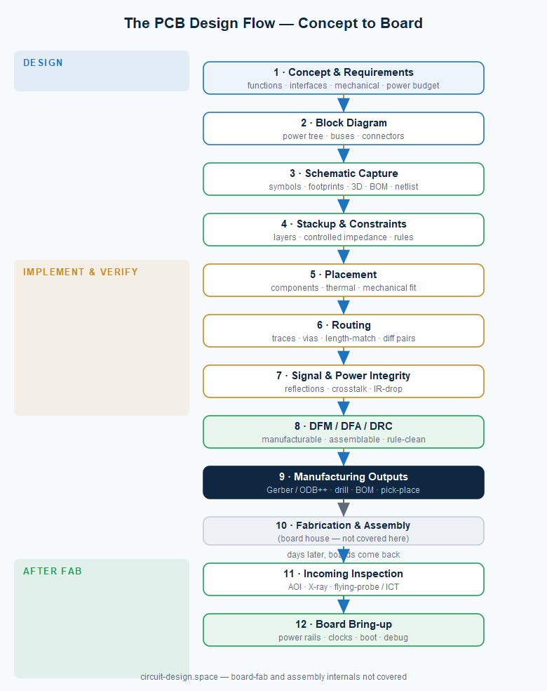
A companion to our walkthrough of the ASIC design flow. That article followed a chip from idea to silicon. This one follows a printed circuit board — the thing those chips get soldered onto — from concept to a fabricated, assembled, powered-up board on the bench. As with the chip flow, we cover the engineering; the physics inside the board-fab and assembly house is its own trade.
A PCB (printed circuit board) is the physical substrate that holds components and wires them together with etched copper. Designing one is its own pipeline — parallel in spirit to chip design, but with different tools, different failure modes, and a much shorter loop back to physical hardware. Below, each step lists what it does, its goal, and the tools, referencing the platforms that dominate professional PCB design: Cadence (Allegro / OrCAD), Siemens EDA (Xpedition / PADS / HyperLynx), Altium Designer, Zuken (CR-8000), and Ansys for signal- and power-integrity analysis.
1. Concept and requirements
What it does. Turns a product need into board-level requirements: what functions the board provides, the key components (processors, power, connectors, sensors), the interfaces and their speeds, mechanical constraints (size, mounting, connector positions), power budget, cost, and environment (temperature, vibration, compliance). For a safety- or reliability- critical board this is also where the hazard and derating requirements are set.
Goal. A clear specification and a rough architecture the rest of the flow can execute against — cheap to change now, expensive to change after layout.
2. Block diagram
What it does. Captures the board as functional blocks and the connections between them — power domains and rails, the main ICs, the high-speed and low-speed buses, clocking, and the external connectors — before drawing a single wire. It’s where the power tree and the interface topology get worked out.
Goal. A partitioning that’s electrically and mechanically sound, so the detailed schematic isn’t fighting a bad architecture.
3. Schematic capture — with libraries and 3D
What it does. Draws the full circuit: every component, every net, every value, on schematic sheets. This step leans heavily on component libraries, and getting them right is half the battle. Each part carries three linked views:
- a schematic symbol (how it appears on the schematic),
- a PCB footprint (the exact copper pads, courtyard, and dimensions the physical part solders to — get this wrong and the board is scrap), and
- a 3D model (so the board can be checked mechanically — height, clearance, connector and mounting-hole alignment against the enclosure).
Modern tools manage these as managed components tied to real manufacturer part numbers and live supply data. The schematic also drives the BOM (bill of materials — the parts list that will be ordered and assembled) and produces the netlist that hands connectivity to layout.
Goal. A complete, correct, reviewable circuit with trustworthy footprints and a clean netlist — the single source of truth the layout must match.
Tools.Cadence OrCAD / Allegro, Siemens PADS / Xpedition, and Altium Designer all provide integrated schematic capture, managed libraries, and linked 3D.
4. Board setup — stackup and constraints
What it does. Before placing anything, define the layer stackup (how many copper layers, their thicknesses, and the dielectric between them) and the design constraints. The stackup determines controlled impedance — the precise trace geometry needed so high-speed signals see a consistent impedance (e.g., 50 Ω single-ended, 100 Ω differential). Constraints capture trace widths, spacings, differential-pair rules, length-matching requirements, and clearances, so the layout tool can enforce them automatically.
Goal. A manufacturable stackup and a constraint set that encodes the electrical intent, so routing is correct by construction rather than by inspection.
5. Placement
What it does. Positions every component on the board. Placement is the single most consequential layout decision: it sets the length and feasibility of every subsequent route, the thermal behavior, the power-delivery path, and the mechanical fit. Connectors and mechanically-fixed parts land first (often driven by the enclosure via ECAD-MCAD co-design), then power, then the high-speed and sensitive analog sections are placed to keep critical nets short and quiet.
Goal. A placement that makes good routing possible, keeps power and heat manageable, and fits the mechanical envelope.
6. Routing
What it does. Draws the actual copper — the traces and vias that connect every net across the layers, honoring the constraints from step 4. High-speed work dominates the effort: length-matching buses so bits arrive together, routing differential pairs with controlled spacing, maintaining reference planes for clean return paths, and managing the copper pours and power planes that deliver current. Low-speed and power nets are routed around them.
Goal. Every net connected, every high-speed rule met, with clean power delivery and return paths — a physically complete board.
Tools.Cadence Allegro X, Siemens Xpedition, Altium Designer, and Zuken CR-8000 are the professional layout environments.
7. Signal and power integrity (SI/PI)
What it does. Verifies the board electrically before it’s built. Signal integrity checks that high-speed signals arrive clean — impedance is controlled, reflections and crosstalk are bounded, and eye diagrams close on multi-gigabit links. Power integrity checks that the power-delivery network holds voltage steady under load — the plane impedance, decoupling, and IR-drop are adequate. On the fastest interfaces this extends to full electromagnetic modeling of the channel.
Goal. Confidence that the board will work at speed, not just connect correctly — before committing to fabrication.
Tools.Siemens HyperLynx and Ansys SIwave / HFSS; Cadence provides integrated SI/PI within the Allegro platform.
Going deeper. This step has a five-part series of its own: signal integrity — the channel, the connector, and which solver to reach for, power integrity — from static IR drop to rapid di/dt, and RF and microwave design, plus on-die signal integrity and silicon power usage for the chip side. Between them they cover the formulas, the decision framework for choosing a solver, and the measurement discipline that keeps a simulation honest.
8. DFM, DFA, and design-rule checks
What it does. The gate before release. DRC (design-rule check) verifies the layout obeys the electrical and spacing rules. DFM (design for manufacturability) checks the board can actually be fabricated reliably — trace/space minimums, annular rings, solder-mask slivers, acid traps, copper balance. DFA (design for assembly) checks it can be assembled — adequate component spacing, correct courtyards, thermal reliefs, fiducials for the pick-and-place machine, and testability access. Catching these here is the difference between a clean build and a scrapped panel.
Goal. A design proven manufacturable and assemblable, not just electrically correct.
Tools. DFM/DFA analysis is built into Siemens, Cadence, and Altium; many teams also run a dedicated DFM check against their fab house’s specific capabilities.
9. Manufacturing outputs — export to the fab house
What it does. Generates the complete data package the board house and assembler consume: the copper, mask, and silkscreen layers as Gerber files (or the richer, single-file ODB++ / IPC-2581 formats), the drill files, the BOM, the pick-and-place (centroid) file that tells the assembly machine where each part goes, the assembly drawings, and the fabrication notes and stackup. This package is the board’s equivalent of a chip’s GDSII handoff.
Goal. A complete, unambiguous manufacturing dataset — so the board that comes back is the board you designed.
10. Fabrication and assembly
The board house etches the copper, laminates the stackup, drills and plates the vias, and applies mask and silkscreen; the assembler then solders the components — stencil, place, reflow. The chemistry and machinery of that are a separate discipline this article doesn’t cover. But engineering resumes the moment the boards come back.
11. Incoming inspection — what comes back
What it does. Before trusting a returned board, verify the build. AOI (automated optical inspection) and, for hidden joints like BGAs, X-ray inspection check that components are present, correct, and well-soldered. Bare-board and assembled electrical tests — flying-probe or ICT (in-circuit test) — check for shorts, opens, and wrong values against the netlist. This screens out fabrication and assembly defects before they waste bring-up time.
Goal. Confidence that a board that fails on the bench failed by design, not by a bad solder joint — so debugging targets the right thing.
12. Board bring-up
What it does. Power the board for the first time — carefully. Bring-up proceeds in order: check power rails come up correctly and in sequence (often current-limited at first), confirm clocks and resets, then boot the firmware and exercise each interface. Problems are localized with the schematic, an oscilloscope and logic analyzer, and the board’s test points and debug headers. Findings feed back: a respin-worthy bug drives a board revision, a fixable one may be patched with a rework wire.
Goal. A board proven to power up, run its firmware, and meet its functional and performance requirements — the payoff of the whole flow.
Optional overlay — the ISO 26262 functional-safety flow for boards
If the board goes into a car — or any system where a malfunction can hurt someone — the flow above is necessary but not sufficient. ISO 26262 (“Road vehicles — Functional safety”) requires a parallel set of board-level activities that run alongside every step, each producing its own evidence, all assembled into a safety case. This is the same discipline our ASIC flow article covers at the chip level, applied to the printed circuit board — the redundancy, monitoring, and component discipline happen in copper and components instead of RTL.
The rigor scales with the ASIL (Automotive Safety Integrity Level), A (least) to D (most stringent). ASIL B and ASIL D are the common targets, and the quantitative bars the hardware must clear differ sharply:
| Metric | What it means | ASIL B | ASIL D |
|---|---|---|---|
| SPFM (single-point fault metric) | fraction of faults covered by a safety mechanism or safe by design | ≥ 90% | ≥ 99% |
| LFM (latent-fault metric) | fraction of undetected faults a second mechanism still catches | ≥ 60% | ≥ 90% |
| PMHF (probabilistic metric for random hardware failures) | residual dangerous-failure rate, in FIT (failures per 10⁹ h) | < 100 FIT | < 10 FIT |
Each activity below notes where it hooks into the standard board flow.
PS1. Item definition, HARA and safety goals(hooks into step 1) — the HARA (Hazard Analysis and Risk Assessment) identifies hazards and rates them on severity, exposure, and controllability, which determines the ASIL and yields the top-level safety goals. Tools:Ansys medini analyze.
PS2. Technical safety requirements allocated to the board(hooks into steps 1–2) — the safety goals are refined into concrete, traceable hardware requirements assigned to specific parts of the board (this rail, this monitor, this redundant channel).
PS3. Safety mechanisms on the board(hooks into step 3, schematic) — the board actively detects and reacts to faults: voltage/current supervisors, a window watchdog, safe-state control (e-fuse, safe shutdown), redundant or diverse-redundant channels, and decoupling/monitoring on critical rails. These are the board-level analogue of a chip’s ECC and lockstep.
PS4. Board-level FMEDA(hooks into steps 3–6) — the FMEDA (Failure Modes, Effects, and Diagnostic Analysis) enumerates each component’s failure modes, assigns base failure rates from reliability handbooks (SN 29500, IEC 62380, or FIDES), credits each safety mechanism with a diagnostic coverage, and rolls the result up into SPFM, LFM, and PMHF to check against the ASIL targets above. Tools: medini analyze; Ansys Sherlock / ReliaSoft for the component FIT data.
PS5. DFMEA, FTA and dependent-failure analysis (DFA)(hooks into step 5, placement) — a board has strong common-cause risks the FMEDA’s independence assumption misses: a shared supply rail, a shared clock, thermal coupling, or two “redundant” parts sitting next to each other. DFMEA, FTA, and DFA hunt these out and drive mitigations — most importantly physical separation on the board for freedom from interference. This is why safety matters so much at placement.
PS6. Component qualification and derating(hooks into step 3, BOM) — safety-relevant parts must be automotive-qualified (AEC-Q100 for ICs, AEC-Q200 for passives, AEC-Q101 for discretes) and used within conservative derating limits (voltage, current, temperature, power) so they stay reliable across the mission profile.
PS7. Reliability and thermal analysis(hooks into steps 5–7) — a physics-of-failure and thermal analysis predicts wear-out mechanisms (solder-joint fatigue, via cracking, electrolytic-cap aging) and confirms every part stays within its thermal derating, feeding the FMEDA’s base failure rates. Tools:Ansys Sherlock for physics-of- failure and thermal.
PS8. Safety validation, confirmation reviews and safety case(hooks in before step 9, fab release) — the evidence — HARA, requirements traceability, board FMEDA, DFA, qualification and derating records, reviews — is assembled into an auditable safety case, with independent confirmation reviews signing it off before release.
The board and the chip share one safety story. The strongest safety case is one where the IP inside the chip already carries its own ISO 26262 work products, so the board-level FMEDA can credit them directly instead of treating each chip as an opaque black box. That’s exactly what our safety soft-IP provides — and we design the safety-aware boards those chips live on.
PCB vs. ASIC: the same shape, a shorter loop
The board flow rhymes with the chip flow — specification, capture, physical implementation, verification, a manufacturing handoff, and bring-up — but two things differ sharply. First, the loop is far shorter and cheaper: a board respin is days-to-weeks and hundreds-to-thousands of dollars, versus months and millions for silicon, so the discipline can be a little more iterative. Second, the physical design is placement-and-routing on a handful of copper layers rather than billions of transistors, so a human designer stays hands-on throughout. Both, though, live or die on the same things: correct libraries/IP, controlled impedance and clean power, and verification before you commit to manufacturing.
Where we fit
We design at both levels — the safety soft-IP that goes inside the chip, and the boards and systems those chips live on: schematic, high-speed layout, signal and power integrity, and bring-up. If you have a board or system that needs to be designed, verified, and brought up — or IP that needs to drop cleanly into one — that’s what we do. See circuit-design.space.
Glossary
AOI — Automated Optical Inspection: camera-based checking of assembled boards for placement and solder defects. Fast and cheap, and blind to anything it cannot see — which is why BGAs and other hidden joints need X-ray instead.
BOM — Bill of Materials: every component, value and part number to be ordered and assembled. Also where a project most often dies quietly — a part that is correct, simulated and unobtainable stops a build as effectively as a design error, so lifecycle status and lead time belong in the BOM review, not after it.
Controlled impedance — Trace geometry engineered so a signal sees a specified, constant impedance, typically 50 Ω single-ended or 100 Ω differential. It is a fabrication requirement as much as a design one: the fabricator adjusts trace width to hit the target with their actual laminate, so the stackup drawing must say which layers are controlled and to what tolerance, usually ±10%.
Copper pour — A filled copper region, typically a power or ground plane. Its value is as a return path, not as a shield: a signal’s return current flows directly beneath it, and a slot or split in the pour that forces that current to detour is one of the most common causes of both signal-integrity and EMC failures.
DFA — Design for Assembly: making the board assemblable reliably — component spacing, courtyards, fiducials, thermal relief on pads connected to planes, orientation consistency. Cheap to get right at layout and expensive to fix once a stencil exists.
DFM — Design for Manufacturability: making the board fabricable reliably — minimum trace and space, annular ring, drill-to-copper, copper balance across the panel. Every fabricator publishes their capability tiers with prices attached, and designing one tier tighter than you need is a straightforward way to pay more and yield less.
Differential pair — Two coupled traces carrying complementary signals. The benefits — common-mode noise rejection, controlled return, lower emissions — all depend on symmetry, so an asymmetry (one via, unequal length, a split under one trace) converts differential energy to common mode, which is what actually radiates.
DRC — Design Rule Check: automated verification that the layout obeys its electrical and spacing rules. Necessary, not sufficient, and only as good as the rules loaded — a clean DRC against default rules on a controlled-impedance board proves very little.
ECAD-MCAD — The link between electrical and mechanical design, exchanged as STEP or IDF. Connectors, mounting holes, tall components and keep-outs are all owned jointly, and the classic failure is a board that is electrically perfect and 2 mm too tall for the enclosure.
Fiducial — A reference mark the pick-and-place machine uses to locate the board optically. Global fiducials locate the panel; local fiducials next to a fine-pitch device locate it, and omitting them on a 0.4 mm-pitch BGA is how placement accuracy quietly becomes a yield problem.
Footprint (land pattern) — The exact copper pads, mask openings, paste apertures and courtyard a physical component solders to. IPC-7351 gives density levels — least, nominal, most — and choosing the wrong one is a common cause of tombstoning at one extreme and unroutable fan-out at the other.
Gerber — The classic per-layer file format handed to the fabricator. X2 adds attributes that identify what each layer is, which removes a whole class of “which file is the top mask?” errors that plain RS-274X leaves to the filename.
ICT — In-Circuit Test: a bed-of-nails fixture that contacts test points to verify components and catch shorts and opens. Needs test points designed in from the start — adding them after layout is a re-spin — and is being displaced on dense boards by boundary scan and flying-probe.
Length matching — Adjusting trace lengths so related signals arrive together. Note it is really delay matching: two traces of equal length on different layers, or over different fibre-weave, do not arrive together, which is why matching is specified within a layer and why serpentines are kept away from the weave direction.
Netlist — The connectivity exported from schematic to layout. The handover point where a schematic error becomes a board error, and the reason schematic review is worth more per hour than layout review.
ODB++ / IPC-2581 — Single-file manufacturing formats carrying stackup, netlist, drill and impedance intent alongside the copper. Both remove the ambiguity of a folder of Gerbers; IPC-2581 is the open standard, ODB++ the widely-supported incumbent.
Pick-and-place (centroid) — The file giving each component’s position, rotation and side for the assembly machine. Rotation convention is the classic trap: a part rotated 90° in the wrong direction assembles an entire panel backwards, and the fix is a first-article check, not a better file.
PI (power integrity) — Analysis that the power delivery network holds voltage steady under load, from static IR drop through decoupling to plane resonance. Covered in depth in power integrity.
Reflow — The soldering process: paste printed through a stencil, parts placed, then the board taken through a thermal profile that melts the solder. The profile is a real design constraint — large copper areas sink heat, so a part on a plane connection without thermal relief can fail to reflow while its neighbour is fine.
SI (signal integrity) — Analysis of reflections, crosstalk, loss and timing on fast signals. Which analysis, and which class of solver, is the subject of this article.
Silkscreen — The printed labels and outlines on the board surface. Purely for humans, and worth the effort: reference designators that are readable after assembly, polarity marks that are not hidden under the part, and connector pin 1 marked where a technician can see it.
Solder mask — The coating that exposes only the pads to be soldered. Mask-defined versus non-solder-mask-defined pads changes the joint geometry and its fatigue life, and the choice is usually dictated by the component vendor rather than free.
Stackup — The arrangement of copper, prepreg and core that makes up the board. It decides impedance, return paths, layer count, cost and how much crosstalk you will have, and it is the single highest-leverage decision in the layout — made first, changed last, and expensive to revisit.
Via — A plated hole connecting copper on different layers. Through, blind, buried and micro; each has a cost and a minimum size. Above a few GHz the unused portion of a through-via is a resonant stub, which is what back-drilling exists to remove.
X-ray inspection — Imaging of hidden joints under BGAs and QFNs. The only way to see a head- in-pillow defect or a void fraction, and the reason a board with a BGA should not go to volume without an X-ray capability somewhere in the process.
Functional-safety terms (ISO 26262)
AEC-Q100 / Q101 / Q200 — Automotive qualification standards for ICs, discrete semiconductors and passive components respectively. They qualify a part against a temperature grade and a stress sequence; they are not a functional-safety claim, and a part being AEC-Q100 qualified says nothing about its FIT rate or its diagnostic coverage.
ASIL — Automotive Safety Integrity Level, A to D, derived in the HARA from severity, exposure and controllability. D is the most stringent. It is a property of the hazard rather than of any component, and it sets the quantitative targets — SPFM, LFM and PMHF — that the hardware must then meet.
Derating — Operating a component well inside its rated limits so that failure rate falls and lifetime rises. Not a rule of thumb but a documented policy: a derating table (typically 50–80% of rating depending on part class) applied consistently and checked at review, because the base failure rates in the analysis assume it.
DFA (safety sense) — Dependent-Failure Analysis: finding the common-cause and cascading failures that defeat redundancy — a shared supply, a shared clock, a shared thermal region, or simply two “redundant” parts sitting next to each other under the same fault. Redundancy that has not been DFA’d is an assumption, not an argument. Note: in layout, DFA also means Design for Assembly.
FIT — Failures In Time: one failure per operating hours. The common unit for component base failure rates and for PMHF, taken from IEC 62380, SN 29500 or the manufacturer, and always scaled by the mission profile’s temperature.
FMEDA — Failure Modes, Effects and Diagnostic Analysis: the quantitative analysis that takes component failure rates, failure-mode distributions and diagnostic coverages and produces SPFM, LFM and PMHF. See the work-package article for what actually ships in one.
Freedom from interference — Assurance that a fault in one element cannot propagate to corrupt another. On a board this is largely physical: separate supplies, separate connectors, spatial separation, and barriers — and it is the argument that lets a lower-ASIL function share a PCB with a higher-ASIL one.
HARA — Hazard Analysis and Risk Assessment: identifies the hazards, rates each for severity, exposure and controllability, and from that assigns the ASIL and states the safety goals. Everything downstream — including every number in the FMEDA — is traceable to it.
ISO 26262 — The automotive functional-safety standard for electrical and electronic systems in road vehicles. Part 5 covers hardware and is where the metric targets live; Part 11 addresses semiconductors specifically.
LFM — Latent-Fault Metric: coverage of faults that are undetected and harmless alone but dangerous in combination with a second fault. Targets 60% / 80% / 90% for ASIL B / C / D. In practice it measures whether your safety mechanisms can themselves be tested.
PMHF — Probabilistic Metric for random Hardware Failures: the whole-item rate of safety-goal violation, in failures per hour. /h for ASIL B and C, /h for D. The only absolute metric of the three, so it is the one that notices when an item is simply too big to be safe at a given coverage.
Safe state — The defined condition the system is driven to when a fault is detected, so the fault does not become a hazard. It has to be reachable from every operating state, within the fault-tolerant time interval, and it must itself be safe — “turn everything off” is not automatically a safe state for a steering system.
Safety case — The assembled, auditable body of evidence arguing the design is acceptably safe: the HARA, the safety requirements, the FMEDA, the verification results, the assumptions of use, and the argument tying them together. It is a document set an assessor reads, not a number.
Safety mechanism — Anything that detects or controls faults so they do not cause a hazard: a supply supervisor, a watchdog, a redundant channel, a CRC, an e-fuse. Each one earns a diagnostic coverage in the FMEDA, and each claim needs evidence — ideally two-sided, where disabling the mechanism is shown to make the metric fall back.
SPFM — Single-Point Fault Metric: the fraction of failure rate that is either covered by a safety mechanism or safe by design. Targets 90% / 97% / 99% for ASIL B / C / D. Sensitive to how the safe fraction was drawn, which is why that split deserves scrutiny.
Further reading — reference books
Book links below are Amazon affiliate links: if you buy through one we earn a small commission at no extra cost to you. It does not influence what is recommended — the same books were on this list before the links were.
- Howard Johnson & Martin Graham, High-Speed Digital Design: A Handbook of Black Magic — the classic on SI and high-speed layout.
- Eric Bogatin, Signal and Power Integrity — Simplified.
- Henry Ott, Electromagnetic Compatibility Engineering — grounding, shielding, EMC.
- Lee Ritchey, Right the First Time: A Practical Handbook on High-Speed PCB and System Design.
- Clyde Coombs & Happy Holden, Printed Circuits Handbook — the encyclopedic reference on fabrication and assembly.
- Mark Montrose, EMC and the Printed Circuit Board.
- ISO 26262:2018, Road vehicles — Functional safety (Parts 5 and 9 for hardware).
Have a board or system to design, verify, or bring up? That’s what we do. Reach us at circuit-design.space.
circuit-design.space · +1-971-357-1400 · anovickis@circuit-design.space