A companion to our walkthrough of the ASIC design flow. That article covered the engineering steps from concept to tapeout. This one explains the thing all of those steps are ultimately designing for: the process geometry — the physical technology a chip is built in. You’ll hear people say “we’re doing this in 5-nanometer” or “we moved to FinFET.” Here’s what that actually means, and why it shapes every decision in the flow.
We still stop at the fab door — this is about understanding the target technology and the geometry your design has to obey, not about running the manufacturing line.
What a “process node” is — and isn’t
A process node is the name for a specific generation of manufacturing technology from a foundry — “180 nm,” “28 nm,” “7 nm,” “3 nm,” and so on. Historically the number referred to a real physical dimension: roughly the smallest feature, or the transistor gate length, you could print. Smaller meant transistors that were faster, lower-power, and packed more densely — the engine of Moore’s Law.
Here’s the catch that trips people up: the nanometer number stopped being a literal measurement years ago. The node name and the actual transistor gate length began diverging in the mid-1990s, and since roughly 2009 the “node” has been a commercial name for a process generation, with no fixed relation to gate length, metal pitch, or gate pitch. At advanced nodes, “5 nm” is a generation label, not a dimension you’ll find anywhere on the chip — no feature on a “5 nm” part is actually 5 nm — and different foundries’ same-named nodes aren’t identical.
For a sense of the cadence, here’s the rough generational timeline (introduction years are approximate and vary by foundry):
| Node | ~Year | Node | ~Year | |
|---|---|---|---|---|
| 180 nm | 1999 | 14 nm | 2014 | |
| 130 nm | 2001 | 10 nm | 2016 | |
| 90 nm | 2003 | 7 nm | 2018 | |
| 65 nm | 2005 | 5 nm | 2020 | |
| 45 nm | 2007 | 3 nm | 2022 | |
| 28 nm | 2010 | 2 nm | ~2025 | |
| 22 nm | 2012 |
Each step roughly follows the historical two-year cadence, and each is a full technology generation — new geometry, new design rules, a new PDK.
What actually matters, and what engineers compare, are the real geometric parameters:
- Contacted poly pitch (CPP) — the spacing between transistor gates.
- Minimum metal pitch (MMP) — how tightly the finest wires can be packed.
- Transistor density — usable transistors per square millimeter.
- Standard-cell track height — how “tall” a logic cell is, in routing tracks.
Those numbers tell you what a node can really do. The headline “nm” is just the label on the box.
The transistor, in three acts
The switch at the heart of every digital chip is the transistor, and its geometry has been reinvented twice to keep scaling alive.
Planar MOSFET (the classic). For decades the transistor was flat: a gate lying over a channel, controlling current from one side. Simple, but as it shrank, the gate lost control — current leaked even when the transistor was “off,” wasting power.
FinFET (introduced at 22 nm, ~2011). Intel demonstrated the first production FinFETs at the 22 nm node: the channel was stood up on its edge into a thin “fin,” and the gate wrapped over it on three sides. More surface contact means far better control, much less leakage, and continued scaling. FinFETs then powered roughly a decade of advanced chips across the industry.
Gate-all-around / nanosheet (GAA, ~2018 onward, now the leading edge). Proposed around 2018 as the successor to FinFET, GAA makes the channel a stack of horizontal sheets with the gate wrapped entirely around each one — control on all four sides. This is the transistor of the newest nodes (the 2 nm generation), squeezing out more performance and efficiency where FinFETs run out of room.
Each transition is a geometry change — a different physical shape for the same logical switch — and it ripples through the design rules, the standard-cell libraries, and the models the whole design flow depends on.
The vertical stack: FEOL and BEOL
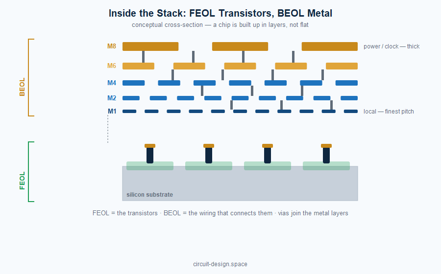
A chip is not flat — it’s a layered structure built up over dozens of steps, and it splits into two regions:
- FEOL — Front-End-of-Line. The bottom: the transistors themselves, formed in and just above the silicon. This is where the fins or nanosheets and their gates live.
- BEOL — Back-End-of-Line. Everything above: the metal stack — many layers of copper wiring (M1, M2, … up to a dozen or more), separated by insulation and connected vertically by vias, that route signals and power across the chip.
The lowest metals are the finest and most tightly pitched (local connections inside cells); the higher metals are progressively thicker and wider (long-distance signals, clock, and power distribution). When you hear that “the wires now dominate delay,” this is why: at advanced nodes, a signal spends more of its time traversing BEOL metal than switching a transistor.
This stack is exactly what the back-end of the design flow produces and verifies: place-and-route fills these metal layers, parasitic extraction measures their real R and C, and physical verification checks the geometry against the foundry’s rules.
Design rules — and why DRC exists
Every foundry publishes a design rule manual: hundreds to thousands of geometric constraints the layout must obey to be manufacturable — minimum widths, minimum spacings, enclosure and overlap requirements, density windows, and many more. These rules exist because you cannot print a shape more precisely than the physics of lithography allows, and because features that are too close, too thin, or too sparse won’t fabricate reliably or will hurt yield.
The design-rule check — DRC — in the flow is the automated enforcement of that manual. When a layout is “DRC-clean,” it means every one of those geometric constraints is satisfied. Its sibling, LVS (Layout Versus Schematic), separately proves the geometry you’re about to build is electrically the circuit you intended. Together they’re the gate before tapeout, and at advanced nodes the rule decks are so complex that a small number of sign-off tools — led by Siemens EDA Calibre, with Synopsys IC Validator and Cadence Pegasus — are trusted to run them.
Lithography, just conceptually
You don’t need to run a fab to understand why geometry is constrained. Chips are patterned by lithography: projecting a mask’s pattern onto the wafer with light. The wavelength of that light sets a floor on how small and how sharp a feature can be printed.
For years, features got smaller than the light’s wavelength through clever tricks — and through multi-patterning, splitting one dense layer across several masks and exposures because a single exposure couldn’t resolve it. That’s expensive and constrains layout (it’s a major reason design rules got so intricate). The move to EUV (extreme-ultraviolet) lithography, with a far shorter wavelength, relaxed some of that pressure at the leading nodes.
The takeaway for a designer: the reason your layout must follow thousands of rules, and the reason advanced nodes are so costly, both trace back to the physics of printing these geometries.
The PDK: the contract with the foundry
You never design against a node in the abstract. You design against its PDK — the Process Design Kit — the package a foundry provides for a given process. The PDK is the formal contract between designer and fab, and it contains:
- the design rules (for DRC),
- the device models (how the transistors behave electrically, for SPICE and timing),
- the standard-cell libraries (pre-designed, pre-characterized logic gates and flip-flops laid out to that node’s geometry),
- and often memory compilers and foundational IP.
Everything in the design flow — synthesis mapping to those cells, timing using those models, DRC using those rules — is anchored to a specific PDK. Choosing a node means choosing a PDK, and committing to its geometry.
Standard cells: where logic meets geometry
The bridge between “logic” and “silicon geometry” is the standard cell. A synthesis tool doesn’t emit transistors; it emits a netlist of standard cells — AND, OR, flip-flop, and hundreds of variants — each a small, pre-designed layout in the target node’s geometry, built to a fixed cell height measured in routing tracks. Because every cell shares that height and a common power-rail arrangement, placement can tile them into rows and route between them.
That’s why “cell height in tracks” and “poly pitch” are the density levers that actually matter: they set how much logic fits per square millimeter, far more meaningfully than the node’s nanometer label.
What this means for your design
Process geometry is not a fab detail you can ignore — it drives the core trade-offs:
- Smaller node → more speed, lower power, higher density — but higher cost and complexity. Mask sets, design effort, and rule-deck difficulty all rise steeply at advanced nodes.
- The right node is the one that fits the product, not the smallest available. Plenty of excellent chips ship on mature nodes (28 nm, 40 nm, 130 nm) where cost, analog performance, or reliability matter more than raw density.
- Analog doesn’t scale like digital. Shrinking the geometry helps digital logic enormously; analog blocks often gain little or even suffer, which is one reason mixed-signal design is hard (see the design-flow article).
MPW — trying a geometry without betting the company
Because a full mask set for an advanced node is so expensive, a multi-project wafer (MPW) shuttle lets you fabricate a prototype in a real process geometry at a fraction of the cost, by sharing the wafer and masks with other designs. It’s the standard way to prove a design in actual silicon — on the actual node geometry — before committing to a dedicated production run.
Where portable IP fits in
Here’s a practical consequence of everything above: geometry is foundry- and node-specific, so IP that’s hard-wired to one foundry’s macros, PLLs, or RAM blocks is painful to move.
We deliberately build our soft-IP as technology-independent, synthesizable RTL — no vendor-specific library cells, no hard PLLs, no foundry RAM macros baked in. That means the same verified block maps cleanly onto your PDK and your chosen node geometry, instead of tying you to one process. Combined with each block’s functional-safety work products, you get IP that ports across nodes as your product roadmap moves. See circuit-design.space.
Glossary
BEOL — Back-End-of-Line: the metal interconnect layers built above the transistors. It has scaled far worse than the transistors have, which is why interconnect resistance and RC delay now dominate performance at advanced nodes — the devices got faster and the wires between them did not.
CPP — Contacted Poly Pitch: the spacing between transistor gates including the contact. One of the two numbers that actually describe a node’s density, and unlike the node name it is a measurable dimension. Density scales roughly as .
Design rules — The geometric constraints a foundry requires for a manufacturable layout. They are not physics; they are the foundry’s statement of what its process can print with acceptable yield, and they get more numerous and more conditional at every node — a modern rule deck runs to thousands of rules, many of them context-dependent.
DRC — Design Rule Check: automated verification that a layout obeys those rules. Clean DRC is necessary and nowhere near sufficient — it says the shapes are printable, not that the circuit works, which is what LVS and timing are for.
EUV — Extreme-Ultraviolet lithography at 13.5 nm wavelength. Its value is that it prints in one exposure what previously needed three or four patterned masks, which recovers both cost and overlay accuracy. The machines are among the most complex objects ever manufactured, and their availability is a real constraint on who can build at the leading edge.
FEOL — Front-End-of-Line: the transistor layers formed in and just above the silicon. Where the device innovations (FinFET, GAA) happen, as opposed to BEOL where the scaling difficulty now lives.
FinFET — A transistor whose channel is a vertical fin gated on three sides. The extra gate control is what stopped short-channel leakage from ending scaling around 22 nm; the cost is that channel width becomes quantised — you get an integer number of fins, not an arbitrary width.
GAA / nanosheet — Gate-All-Around: stacked horizontal channels gated on all four sides. The successor to FinFET, with better electrostatic control still, and it restores continuous width selection because the sheet can be drawn wider rather than replicated.
Lithography — Patterning the wafer by projecting a mask image onto photoresist. Resolution follows , which is why the industry has pushed on all three terms: shorter wavelength (EUV), higher numerical aperture (immersion, then High-NA), and better process control to lower .
LVS — Layout Versus Schematic: proof that the physical layout implements the intended circuit. Together with DRC it is the minimum bar for tape-out, and an LVS mismatch late in a project is one of the more expensive things to find.
Metal stack — The set of BEOL wiring layers and the vias connecting them, typically thin and dense at the bottom, thick and sparse at the top. The allocation is a design decision: thin layers for local routing, thick top metal for clocks, power and anything where resistance or inductance matters.
MMP — Minimum Metal Pitch: the tightest spacing of the finest wires. The second real density metric alongside CPP, and the one that governs routability rather than transistor count.
MOSFET — The basic transistor switch. Worth keeping the name in mind because the “MOS” — metal-oxide-semiconductor — has been historically inaccurate since gates went back to metal over high-k dielectric rather than polysilicon over silicon dioxide.
MPW — Multi-Project Wafer: a shared shuttle run where several designs share one mask set and wafer lot. Turns a mask cost of hundreds of thousands into tens of thousands, which is what makes prototyping and academic silicon possible at all.
Multi-patterning — Splitting one dense layer across multiple masks and exposures to print features finer than a single exposure can resolve (LELE, SADP, SAQP). Costs masks, cycle time and overlay budget, and it constrains layout: the decomposition must be colourable, which becomes a design rule of its own.
Node — A generation of manufacturing process, named “7 nm”, “5 nm”, “3 nm”. Since roughly the 28 nm generation the name has been a marketing label rather than a physical dimension; nothing on a 5 nm chip measures 5 nm. Compare CPP, MMP and track height instead, or density in millions of transistors per mm².
PDK — Process Design Kit: the foundry’s package of design rules, device models, extraction decks and standard-cell libraries for a node. Under NDA, node-specific, and the thing that actually determines whether a design can be moved between foundries.
Planar MOSFET — The classic flat transistor, gated from one side only. Still the right choice for most analog, RF, power and mature-node work; it did not become obsolete, it stopped scaling.
Standard cell — A pre-designed, pre-characterised gate or flip-flop laid out to the node’s geometry, with a fixed height so cells abut in rows. The unit synthesis targets, and the reason digital design can be automated at all.
Track (cell height) — Standard-cell height expressed in routing pitches. Fewer tracks means smaller, denser, slower cells; more tracks means faster and larger. Offering several track heights on one node is how a foundry sells density and performance from the same process.
Via — A vertical connection between two metal layers. Individually tiny and collectively decisive: via resistance is a large share of interconnect resistance at advanced nodes, and via reliability (electromigration, voiding) is why design rules insist on redundant vias wherever the layout can afford them.
Further reading — reference books
Book links below are Amazon affiliate links: if you buy through one we earn a small commission at no extra cost to you. It does not influence what is recommended — the same books were on this list before the links were. Standard texts on device geometry, process technology, and layout:
Devices and CMOS geometry
- Weste & Harris, CMOS VLSI Design: A Circuits and Systems Perspective — geometry, standard cells, and layout in the broader VLSI context.
- Sze & Ng, Physics of Semiconductor Devices — the reference on how transistors work.
- Taur & Ning, Fundamentals of Modern VLSI Devices — scaling, short-channel effects, and FinFET/GAA physics.
Process technology and manufacturing
- Plummer, Deal & Griffin, Silicon VLSI Technology: Fundamentals, Practice and Modeling.
- May & Spanos, Fundamentals of Semiconductor Manufacturing and Process Control.
- Xiao, Introduction to Semiconductor Manufacturing Technology.
- Wolf & Tauber, Silicon Processing for the VLSI Era (multi-volume, encyclopedic).
Layout and design rules
- Baker, CMOS: Circuit Design, Layout, and Simulation — hands-on layout and the rules behind it.
- Clein, CMOS IC Layout: Concepts, Methodologies, and Tools.
Node-generation years and the history of node naming draw on Wikipedia’s Semiconductor device fabrication article; specifics vary by foundry.
Choosing a node, porting IP across processes, or want blocks that aren’t welded to one foundry’s geometry? That’s what we build. Reach us at circuit-design.space.
circuit-design.space · +1-971-357-1400 · anovickis@circuit-design.space