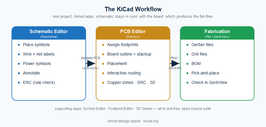
Our PCB design flow article covered the board flow in the abstract, across the commercial tools. This one does it concretely in KiCad — the free, open-source, cross-platform EDA suite — so you can see the whole loop, from a blank project to a set of fabrication files, in one specific toolchain. It’s a map of the workflow, not a click-by-click manual; the official KiCad docs have the button-level detail.
KiCad has matured into a genuinely professional tool — it’s used for everything from hobby boards to shipping products — and because it’s free and open-source, it’s the fastest way to learn the flow hands-on. It’s really a set of linked applications sharing one project: the Schematic Editor (historically Eeschema), the PCB Editor (Pcbnew), the Symbol and Footprint Editors, a 3D Viewer, and a Gerber Viewer (GerbView).
1. Create the project
Open KiCad and start a new project. You get a project file that ties together a schematic and a board, plus library tables. KiCad ships with large, well-maintained official symbol, footprint, and 3D-model libraries, so most common parts are already available — and you can add your own or manufacturer-supplied libraries.
Goal. One project holding the schematic, the board, and their linked libraries.
2. Draw the schematic (Schematic Editor)
Open the Schematic Editor and capture the circuit: place symbols from the libraries, wire them together with the Wire tool, and give nets meaningful names with labels (a label is often cleaner than a drawn wire for buses and power). Use the dedicated power symbols (VCC, GND, +3V3, …) to define rails — nets with the same power symbol connect automatically. For anything bigger than a page, split across hierarchical sheets.
When the drawing is done, annotate it (assign each part a unique reference like R1, U3), then run ERC — the Electrical Rule Check. ERC catches the classic mistakes: unconnected pins, outputs shorted together, a power input with no source. Clear the ERC before moving on; it’s much cheaper than finding the same error on the bench.
Goal. A complete, annotated, ERC-clean schematic — the single source of truth for the board.
3. Assign footprints
Every symbol needs a footprint — the physical pads and outline the real part solders to. In KiCad you assign these with the footprint-assignment tool (historically CvPcb, now built into the schematic flow), matching each symbol to a library footprint. This is the step to be careful with: a wrong footprint (wrong pin pitch, wrong package) is one of the most common ways a first board turns into scrap. Where available, the assigned footprint also links a 3D model for the mechanical check later.
Goal. Every part mapped to the correct physical footprint, verified against the real component’s datasheet.
4. Push the schematic into the board
In modern KiCad you don’t export a separate netlist file — you open the PCB Editor and run Update PCB from Schematic. KiCad pulls in every component with its footprint and the full connectivity, dropping the parts onto the board with a ratsnest (the thin lines showing which pads still need to be connected). From here on, the schematic and board stay in sync: change the schematic, re-run the update, and the board follows.
Goal. All footprints on the board, connectivity loaded, ready to lay out.
5. Set up the board
Before placing, define the board itself. Draw the board outline on the Edge.Cuts layer (KiCad can also pull an outline from mechanical CAD). Open Board Setup to configure the layer stackup (how many copper layers), and the design rules: net classes with their track widths and clearances, differential-pair rules, and via sizes. Encoding the rules here lets the router and the design-rule check enforce them for you.
Goal. A defined board shape and a rule set that captures your electrical intent.
6. Place the components
Arrange the parts on the board. Placement drives everything downstream — route length, thermal behavior, power delivery, and mechanical fit — so it’s worth the time. Lock down connectors and any mechanically-fixed parts first (the 3D Viewer and STEP export help you check fit against an enclosure), then group circuitry by function, keep decoupling capacitors tight to their ICs, and keep sensitive analog and high-speed sections short and separated.
Goal. A placement that makes clean routing possible and respects the mechanical and thermal constraints.
7. Route the board
Now draw the copper. KiCad’s interactive router supports walk-around and push-and-shove routing, so tracks nudge existing ones aside as you go. Add vias to change layers, use the differential-pair router for high-speed pairs, and the length-tuning tools to match critical buses. Fill ground and power planes with copper zones (pours), which also give high-speed signals a clean return path. Route power and ground deliberately — plane continuity matters as much as the signal traces.
Goal. Every net in the ratsnest connected, high-speed rules met, solid power and ground.
8. Check it — DRC and 3D
Run the DRC (Design Rule Check) in the PCB Editor. It flags clearance violations, unrouted or unconnected nets, track-width problems, and courtyard overlaps against the rules you set in Board Setup. Fix everything — a clean DRC is the gate before you generate manufacturing files. Then open the 3D Viewer for a visual and mechanical sanity check: component collisions, connector alignment, silkscreen over pads, board fit.
Goal. A DRC-clean, mechanically-sane board you’re confident to build.
9. Generate the fabrication outputs
This is where KiCad produces the package the board house needs:
- Gerbers — from Plot (File → Plot), select the copper, mask, silkscreen, and edge layers. (KiCad can also emit the newer, single-file formats.)
- Drill files — the companion Generate Drill Files dialog.
- BOM — the bill of materials, exported from the schematic.
- Pick-and-place — the component position (centroid) file for the assembly machine (Fabrication → generate position file).
Before sending anything, open the Gerbers in GerbView (or your fab’s online viewer) and look at them — it’s the last chance to catch a wrong layer or a missing polygon. Many fabricators also provide a KiCad plugin (for example a “Fabrication Toolkit”) that bundles all of these in one click to their spec.
Goal. A complete, verified manufacturing dataset — Gerbers, drill, BOM, and placement — ready to upload.
10. Order, then bring it up
Upload the package to a board house, and days later the boards arrive. From there it’s the same bring-up discipline as any board: check the power rails come up correctly (current-limited at first), confirm clocks and resets, then load firmware and exercise each interface, using your test points and a scope to localize anything that misbehaves. KiCad’s schematic and 3D views are your map while you debug.
Goal. A working, powered-up board — and, usually, a short list of tweaks for the next revision.
Why KiCad is a great place to learn the flow
Every concept in our PCB design flow article — schematic capture, libraries and footprints, stackup and constraints, placement, routing, SI-aware layout, DRC, and the Gerber/drill/BOM/pick-and-place handoff — is present in KiCad, in a tool anyone can install for free. The workflow transfers directly to the commercial platforms; the discipline is identical. It’s the fastest way to go from “I understand the theory” to “I’ve shipped a board.”
If you’re taking a board from KiCad prototype to a manufacturable, verified product — or you need high-speed layout, signal- and power-integrity sign-off, or bring-up help — that’s what we do. See circuit-design.space.
Quick reference — the KiCad loop
| Stage | KiCad tool / action |
|---|---|
| Schematic | Schematic Editor → place symbols, wire, annotate, ERC |
| Footprints | Footprint assignment (symbol → footprint) |
| Sync to board | Update PCB from Schematic (no netlist file needed) |
| Board setup | Edge.Cuts outline, Board Setup (stackup, net classes, rules) |
| Layout | Placement, interactive router, diff pairs, length tuning, copper zones |
| Verify | DRC, 3D Viewer |
| Manufacturing | Plot Gerbers, Drill files, BOM, position file; check in GerbView |
The official KiCad documentation and the “Getting Started in KiCad” guide walk through each of these at the button level.
Glossary
Annotation — Assigning reference designators (R1, C4, U2) to symbols. KiCad will not let you proceed without it, because the designator is how the schematic and the board identify the same part to each other.
Edge.Cuts — The layer defining the board outline. Everything mechanical follows from it, and a board with no Edge.Cuts is a board the fabricator cannot make.
ERC / DRC — Electrical Rule Check on the schematic (unconnected pins, output-driving-output, power pins with no source) and Design Rule Check on the board (clearance, width, via, courtyard). Both are necessary and neither says the circuit is correct.
GerbView — KiCad’s Gerber viewer. Open your own output in it before sending it: it is the cheapest possible check that the layers you think you plotted are the ones you plotted.
Net class — A group of nets sharing width, clearance and via rules — power, high-speed, default. Setting these up in Board Setup is what makes the router enforce your intent rather than your vigilance.
Position file (centroid) — Component positions and rotations for the pick-and-place machine. Rotation convention is the classic trap, and the fix is a first-article check rather than a better file.
Update PCB from Schematic — KiCad’s forward-annotation step. It replaces the old netlist file entirely, which is why a KiCad tutorial written before v6 will send you looking for a file that no longer exists.
Zone (copper pour) — A filled copper region, usually a ground plane. Needs refilling after edits — an unfilled zone looks connected on screen and is not.
Further reading
Book links below are Amazon affiliate links: if you buy through one we earn a small commission at no extra cost to you. It does not influence what is recommended — the same books were on this list before the links were.
- The official KiCad documentation — genuinely good, and the fastest route to the button-level detail this article deliberately skips.
- Henry Ott, Electromagnetic Compatibility Engineering — the book on grounding, return paths and why boards fail EMC. Applies to any tool.
- Howard Johnson and Martin Graham, High-Speed Digital Design: A Handbook of Black Magic — where the rise-time rules of thumb come from.
- Our own PCB design flow walkthrough for the tool-independent version of this loop, and signal integrity for when the traces stop being wires.
Building a board in KiCad and want it reviewed, sped up, or brought to production quality? Reach us at circuit-design.space.
circuit-design.space · +1-971-357-1400 · anovickis@circuit-design.space