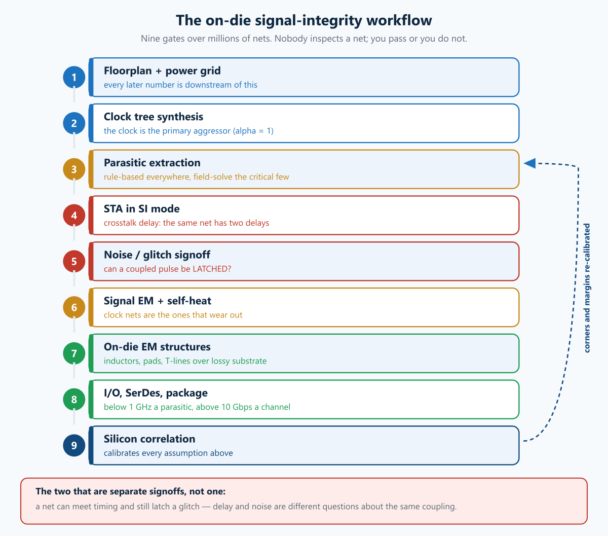
Part four of a series. Parts one to three covered the board: signal integrity and solver choice, power integrity, and RF and microwave. This part and part five on silicon power move inside the die, where the same physics produces a completely different workflow.
Board SI and on-die SI share their physics and almost nothing else. On a board you manage reflections on transmission lines; on a die, almost nothing is a transmission line. A minimum-width wire in a lower metal layer is a resistor with capacitance — its delay is RC, not propagation, and the tools, the failure modes and the signoff criteria all follow from that one fact.
The other difference is scale. A board has hundreds of nets you can reason about individually. A block has millions, and no human looks at any of them. On-die SI is therefore not an analysis you perform, it is a gate you pass, run over an entire netlist, and the workflow below is what that gate is made of.
1. Why on-die wires behave differently
The wire is a resistor
A board trace has negligible series resistance at DC and gets its behaviour from L and C. An on-die wire has enormous resistance, because it is tiny. Delay for a distributed RC line is the Elmore-style approximation:
With illustrative geometries — real numbers depend heavily on the node, and barrier/liner layers plus electron surface scattering push effective resistivity well above bulk copper at advanced nodes:
| Layer class | W × T | Length | R | C | 0.38·RC |
|---|---|---|---|---|---|
| Thin local | 50 nm × 100 nm | 50 µm | 168 Ω | 10 fF | 0.64 ps |
| Intermediate | 100 nm × 200 nm | 100 µm | 84 Ω | 20 fF | 0.64 ps |
| Thick top metal | 400 nm × 800 nm | 1000 µm | 52 Ω | 200 fF | 3.99 ps |
The two thin rows landing on the same delay is a coincidence of the numbers chosen, and a useful one: it shows the trade the metal stack exists to make. Halving the cross-section doubles R; halving the length halves C. Same delay, different reach.
And delay grows with the square of length
Both R and C are proportional to length, so unbuffered RC delay goes as :
| Length | Relative unbuffered delay |
|---|---|
| 100 µm | 1× |
| 200 µm | 4× |
| 400 µm | 16× |
| 1000 µm | 100× |
That quadratic is the entire justification for repeater insertion. Breaking a long wire into segments with buffers converts an L² problem into a linear one, at the cost of area, power and — importantly for this article — a great many more nodes that can be attacked by crosstalk.
When inductance finally matters
Most on-die wires are safely RC. Inductance becomes relevant when resistance falls low enough that the line starts behaving like a transmission line. A workable criterion is to compare the wire’s resistance against its characteristic impedance:
| Wire | Verdict | ||
|---|---|---|---|
| Thick top-metal clock spine | 50 Ω | 100 Ω | inductive — model it |
| Intermediate signal | 500 Ω | 100 Ω | RC-dominated |
| Thin local wire | 2000 Ω | 100 Ω | RC-dominated |
So inductance is a top-metal concern: clock spines, wide power straps, global buses and the top-layer routing of SerDes and RF blocks. Everywhere else, extracting L is wasted effort. Knowing which is which is what keeps extraction runtimes survivable.
2. The workflow
Step 1 — Floorplan and the power grid, before any SI
What it does. Fixes block placement, the metal stack allocation, and the power grid geometry.
Why it is an SI step. Every later SI number is downstream of decisions made here. The power grid consumes routing resource on the same layers signals want; a denser grid means a quieter supply (part two) and a more congested router, which means longer detours, which means more coupling. The choice of which layers are “thick” sets where inductance matters and where long global routes are even possible.
Goal. A floorplan where the critical global nets have a straight path on a layer that can carry them, and a grid dense enough that IR drop does not eat the timing budget.
Tools. Implementation and grid construction — Cadence Innovus, Synopsys Fusion Compiler / IC Compiler II, Siemens Aprisa. Early grid analysis — Ansys RedHawk-SC, Cadence Voltus, Siemens mPower.
Step 2 — Clock tree synthesis, with SI in mind
What it does. Builds the clock distribution: spines, meshes or trees, with balanced insertion delay.
Why it is special. The clock is the most SI-sensitive net on the die and the most dangerous aggressor. It has the highest activity factor of anything (it toggles every cycle by definition), the largest drivers, and it runs everywhere. A clock net that couples into a data net injects noise at exactly the wrong moment; a data net that couples into the clock produces jitter that shows up as timing failure somewhere else entirely.
Goal. Balanced skew, controlled slew, and physical isolation — shielding critical clock routes with grounded neighbours, or at minimum keeping them off layers where long parallel data routes run.
Tools. The same implementation tools build the tree — Cadence Innovus, Synopsys Fusion Compiler. Skew and slew are signed off in PrimeTime / Tempus, and a clock mesh is usually confirmed in SPICE (HSPICE, Spectre) because a mesh is an analog structure that STA models only approximately.
Step 3 — Parasitic extraction
What it does. Converts the routed layout into an electrical netlist: R, C and (selectively) L for every net and every coupling capacitor between neighbours. Output is SPEF or its equivalent.
Two fidelities, and knowing when to use which is the whole skill.Rule-based or pattern-matched extraction matches local geometry against a pre-characterised library. It is fast enough to run over a whole block and is what you use by default. Field-solver extraction actually solves the local field problem and is reserved for nets where the answer matters more than the runtime: clocks, critical timing paths, sensitive analog, high-speed I/O.
The decision that costs projects. Corner selection. Parasitics vary with process — a “C-worst” corner maximises coupling capacitance and hurts crosstalk; “RC-best” makes wires fast and can worsen hold timing. Extracting one corner and hoping is how a chip passes signoff and fails silicon.
Tools. Synopsys StarRC, Cadence Quantus, Siemens Calibre PEX.
Step 4 — Static timing analysis, in SI mode
What it does. Checks every path against setup and hold, at every corner — with crosstalk included.
Why SI-mode STA is a different analysis. A victim net’s delay depends on what its neighbours are doing at that instant. The effective coupling capacitance the victim sees is scaled by a switching factor:
| Aggressor behaviour | Effective coupling cap |
|---|---|
| Quiet | 1.0 × |
| Switching in the same direction | ~0 × |
| Switching in the opposite direction | 2.0 × |
| Worst-case bound used by some flows | up to 3.0 × |
So the same physical net has two different delays depending on its neighbourhood, and the analysis has to consider both: the slow case for setup, the fast case for hold. This is why an SI-mode run finds violations a plain STA run does not, and why turning SI off to “get a clean report” is self-deception.
The tools narrow this with timing windows — an aggressor can only hurt a victim if they can switch at overlapping times — and iterate, because changing a delay changes the windows. Convergence is not guaranteed and a flow that has not converged is not signed off.
Tools. Synopsys PrimeTime SI, Cadence Tempus.
Step 5 — Noise and glitch signoff
What it does. Separately from delay, checks whether a coupled pulse can be large enough and long enough to be latched as data.
The two failure modes. A glitch on a static node that propagates and gets captured. And noise on a node that is not being driven — a floating or weakly-held net, a dynamic-logic node, a pass-gate output — where there is nothing to fight the injected charge. Dynamic logic and latch-based designs are far more exposed than fully static CMOS, which is one of several reasons most digital logic is fully static.
Goal. Every node’s worst-case noise bump below the receiving gate’s noise margin, with the propagated-noise path checked as well as the injected one.
Tools. Synopsys PrimeTime SI and Cadence Tempus do noise and glitch signoff alongside SI-mode timing. Both need noise-aware library models (CCS-N or ECSM-N) from characterisation — Synopsys SiliconSmart, Cadence Liberate — and a library characterised without them silently degrades the analysis to a cruder model.
Step 6 — Signal electromigration and self-heat
What it does. Checks that signal wires carry their switching current without wearing out, using the same Black’s-equation physics as the power grid (part two) but with RMS and peak-current limits rather than DC average.
Why clocks are the risk. Switching current on a net is roughly I = α·C·V·f, so the worst nets are the ones with high capacitance and maximum activity:
| Net | C | Frequency | Switching current (α = 1) |
|---|---|---|---|
| Local net | 50 fF | 2 GHz | 80 µA |
| Long bus | 500 fF | 2 GHz | 800 µA |
| Clock leaf group | 2000 fF | 1 GHz | 1600 µA |
With EM limits on thin metal in the low hundreds of microamps, a clock net is the one that fails — it is the only net with α = 1 by construction. Self-heat compounds it: current through a resistive wire raises that wire’s own temperature above the die average, and the EM lifetime is exponential in temperature.
Tools. Signal EM and self-heat — Cadence Voltus-XFi, Ansys RedHawk-SC and Totem (for analog), Siemens mPower. Rule-based reliability checks that catch the structural cases — Siemens Calibre PERC.
Step 7 — On-die electromagnetic structures
What it does. Field-solves the things that genuinely radiate or resonate: inductors, transformers, top-metal transmission lines, ESD structures, pads and seal rings.
Why it is a separate tool. These are 3D EM problems sitting on a lossy conductive substrate that couples everything to everything. Nothing about them is quasi-TEM and no extraction tool models them properly.
Tools.EMX, HFSS, ADS Momentum.
Step 8 — I/O, SerDes and package co-simulation
What it does. Extends the analysis outward through bumps, redistribution layers, substrate vias and balls, into the board channel.
Why it cannot be skipped above about 10 Gbps. The package is not a wire. It has real discontinuities, and the transmitter’s behaviour depends on the impedance it sees looking out through it. Below roughly a gigahertz the package is a lumped parasitic and quasi-static extraction (Q3D, SIwave) gives you the L and C you need. Above it, the package is a channel, and only full-wave (HFSS, Clarity) tells the truth. Teams get this wrong in both directions — see the chip-side tool map in part one.
Goal. A cascaded model from the driver’s output stage to the receiver’s input, so the eye is simulated through the real path rather than the one the evaluation board happened to have.
Tools. Package and interposer extraction — Ansys HFSS and SIwave, Cadence Clarity and Sigrity, Siemens HyperLynx. The analog front end in HSPICE or Spectre; the statistical channel in an IBIS-AMI flow. Which of those you need is the same decision as on the board — see which solver to reach for.
Step 9 — Silicon correlation
What it does. Compares what the chip actually does against what the flow predicted.
What you have to work with. On-die process monitors and ring oscillators for speed; eye-monitor circuits inside SerDes receivers that report margin directly from the link; scan and BIST for functional failures; and, when something is genuinely mysterious, focused ion beam and probing.
Why it belongs in the workflow and not after it. The extraction corners, the noise margins and the switching-factor assumptions are all models. Correlating one design properly tells you whether they were right, and that calibration is what makes the next design’s signoff trustworthy.
Tools. Not EDA either. A real-time oscilloscope and TDR/TDT for the I/O, a VNA for the package, on-die ring oscillators and eye monitors for anything you cannot probe, and the scan chain for everything else. The correlation itself goes back into the extraction and timing decks as a derate — which is the deliverable, not the waveform.
3. Corners, modes, and why the matrix explodes
None of the above is run once. It is run across MMMC — multi-mode, multi-corner:
- Modes: functional, test/scan, low-power, boot, each with different clocks and constraints.
- PVT corners: process (slow/typical/fast), voltage (nominal and drooped), temperature (cold and hot — and cold is not automatically the fast case once temperature inversion kicks in at low voltage).
- Extraction corners: C-worst, C-best, RC-worst, RC-best, and their temperature variants.
The product of those is hundreds of scenarios, most of which are redundant. Real flows prune to a dominant set and justify the pruning — and that justification is exactly what an independent reviewer should ask to see, because an unjustified prune is how a corner that mattered gets dropped.
4. The tools
| Step | Tool | Note |
|---|---|---|
| Implementation, power grid, CTS | Innovus, Fusion Compiler / ICC2, Aprisa | Where the SI problem is created, not found |
| Grid analysis | RedHawk-SC, Voltus, mPower | Same engines as the EM signoff below |
| Extraction (rule-based) | StarRC, Quantus, Calibre PEX | The default; fast enough for a whole block |
| Extraction (field-solve) | The same tools in solver mode | Critical nets only |
| STA with crosstalk | PrimeTime SI, Tempus | The gate; must converge |
| Noise / glitch | PrimeTime SI, Tempus, Voltus-family noise | Separate from delay |
| Signal EM / self-heat | Totem, RedHawk-SC, Voltus | Same engines as power-grid EM |
| On-die EM structures | EMX, HFSS, Momentum | Lossy substrate, genuine 3D |
| Package RLCG | Q3D, SIwave, Sigrity | Below ~1 GHz: a number |
| Package as channel | HFSS, Clarity | Above ~10 Gbps: a behaviour |
| Circuit / transient | HSPICE, Spectre | The arbiter |
| Link simulation | ADS, Nexxim, IBIS-AMI | Eye and margin |
| Library noise models | SiliconSmart, Liberate | CCS-N / ECSM-N; without them the noise analysis quietly degrades |
| Silicon correlation | Scope, TDR/TDT, VNA, on-die monitors | Not EDA — and the deliverable is a derate, not a waveform |
Two notes on reading that table. The first two rows are not analysis tools, and they are there deliberately: floorplan, grid and clock-tree decisions create the SI problem that everything below then measures, and no amount of signoff recovers a bad one. And the same engines appear under several steps — RedHawk-SC and Voltus do grid IR, dynamic droop and signal EM; PrimeTime SI and Tempus do both delay and noise — so the licence count is smaller than the row count suggests, and the flow decision is usually which vendor stack rather than which product.
5. Best practices
- Extract the right corners, not one corner. C-worst for crosstalk-driven setup, RC-best for hold. A single-corner extraction is not a signoff.
- Never turn SI mode off to clean up a report. The violations do not go away, they just stop being visible.
- Check that SI-mode STA converged. Delay changes move timing windows, which change delay. A non-converged run is a guess.
- Shield the clock, and treat it as the primary aggressor. It is the only net with α = 1.
- Field-solve the few nets where it matters, and let rule-based extraction carry everything else. Doing it everywhere is unaffordable; doing it nowhere is negligent.
- Do not extract inductance where it cannot matter. Use the criterion — on thin metal it is wasted runtime that buys nothing.
- Treat noise and delay as separate signoffs. A net can pass timing and still latch a glitch.
- Watch the clock nets for EM, not the data nets.
- Extract the package and simulate the driver through it, not into an ideal load.
- Correlate one design end to end. It is what calibrates every assumption above.
The pitfalls that cost the most time
- Signing off on a single extraction corner.
- A non-converged SI-mode timing run reported as clean.
- Assuming cold is the fast corner (temperature inversion says otherwise at low voltage).
- Ignoring self-heat on high-activity nets.
- Modelling the package quasi-statically for a 25 Gbps SerDes.
- Simulating the driver into a lumped load instead of the extracted channel.
- Dynamic logic or pass-gate nodes signed off with static-CMOS noise margins.
- Pruning the MMMC matrix without writing down why.
Where we fit
Our primary work is board-level — schematic, layout, stackup, and the signal- and power-integrity analysis around it, in Cadence Allegro, Altium, Ansys SIwave and HFSS, and Siemens HyperLynx — and, where a programme needs it, the FMEDA and FMEA evidence alongside. Silicon and package work sits next to that rather than replacing it: the boundary where a die’s I/O meets a package and then a board is exactly where the two disciplines meet, and it is where most of the interesting failures live.
If you have a link that closes in simulation and not on the bench, or a package transition nobody has modelled properly, that is the conversation we like having.
Glossary
Black’s equation — The electromigration wear-out model, with . Lifetime falls with the square of current density and exponentially with temperature, so a wire that is 10 °C hotter than modelled loses roughly half its life. It is why current-density rules exist on power straps and why self-heat is checked separately from the die’s average temperature.
Coupling capacitance () — Capacitance between two neighbouring wires. As geometries shrank, wires got taller relative to their spacing, so became the dominant component of a net’s capacitance rather than a correction — which is why on-die crosstalk went from a curiosity to a signoff gate.
Elmore delay — The first-order RC delay approximation, for a distributed line. Fast enough to run inside a placer’s inner loop, and always optimistic on slow edges — useful for ordering candidate routes, never for signing off a path.
Glitch (noise bump) — A pulse coupled onto a quiet node. Harmless on a combinational net that settles before it is sampled, dangerous on anything latching or asynchronous — a clock enable, a reset, an SRAM control line — where it can be captured as real. This is the distinction between a noise number and a noise failure.
MMMC — Multi-Mode Multi-Corner: the matrix of functional modes crossed with PVT corners a signoff must run. The count multiplies fast (modes × corners × RC corners), and it is the main reason signoff takes days rather than hours.
Noise margin — How large a disturbance a gate input tolerates before its output responds. Not a single number: it depends on the input slew and the state the gate is holding, which is why modern flows use noise models (CCS-N / ECSM-N) rather than a fixed millivolt budget.
Repeater — A buffer inserted into a long wire. Unbuffered RC delay grows as because both R and C scale with length; cutting the wire into segments makes it , so delay becomes linear in length at the cost of buffer area and power. The reason a modern die contains millions of them.
SI-mode STA — Static timing analysis with crosstalk-induced delay included: an aggressor switching with a victim speeds it up or slows it down depending on direction. Adds delta-delay on top of the nominal path and turns timing closure into a problem that depends on what the neighbours are doing.
Self-heat — A wire raising its own temperature with its own current, above the die average. Matters because Black’s equation is exponential in temperature, and because a thin high-current wire is exactly where both the current density and the thermal resistance are worst.
SPEF — Standard Parasitic Exchange Format: how extraction hands resistance and capacitance to the timing tool. Its coupling capacitors are what make SI-mode STA possible; a flow that collapses them to ground (“lumped” SPEF) runs faster and cannot see crosstalk at all.
Switching factor / MCF — The multiplier applied to coupling capacitance to represent what the aggressor is doing: 0 if it holds, 1 if it is quiet, 2 if it switches the opposite way, sometimes bounded at 3 for safety. Choosing it is choosing how pessimistic your timing is, and a flow that uses 2 everywhere will never close.
Temperature inversion — At low supply voltage, threshold-voltage reduction outweighs mobility degradation, so devices get faster as they get hotter. The cold corner stops being the fast corner, and any flow that assumes otherwise signs off the wrong extreme.
Timing window — The interval during which a net can switch. An aggressor whose window does not overlap the victim’s cannot affect it, so window analysis removes enormous pessimism — and is iterative, because changing a delay changes the windows that produced it.
Further reading — reference books
Book links below are Amazon affiliate links: if you buy through one we earn a small commission at no extra cost to you. It does not influence what is recommended — the same books were on this list before the links were.
- Weste & Harris, CMOS VLSI Design: A Circuits and Systems Perspective — the interconnect and noise chapters are the right starting point.
- Bhasker & Chadha, Static Timing Analysis for Nanometer Designs — including the SI chapters.
- Kahng, Lienig, Markov & Hu, VLSI Physical Design: From Graph Partitioning to Timing Closure.
- Rabaey, Chandrakasan & Nikolić, Digital Integrated Circuits: A Design Perspective — the interconnect and wire-delay treatment.
- Stephen Hall & Howard Heck, Advanced Signal Integrity for High-Speed Digital Designs — for the package and channel end of the problem.
- Eric Bogatin, Signal and Power Integrity — Simplified — the board-side companion.
Have a die, a package, or the boundary between them that needs to work the first time? That’s what we do. Reach us at circuit-design.space.
circuit-design.space · +1-971-357-1400 · anovickis@circuit-design.space