Part five of a series. Part two covered power integrity — delivering the voltage. This part covers the other half of the same problem: how much power the chip draws in the first place, and the workflow that estimates, budgets and reduces it. Part four covered on-die signal integrity.
Power integrity asks whether the voltage holds. Power usage asks how much current is being drawn, and that question is answered much earlier and much less precisely.
The uncomfortable truth of this workflow is that the number depends on what the chip is doing, and nobody knows what the chip will be doing until long after the decisions that determine its power have been made. Every technique below is a way of managing that uncertainty rather than eliminating it.
1. Where the power goes
Three components, two that matter:
Dynamic power — charging and discharging capacitance
α is the activity factor (what fraction of clock cycles a node toggles), C the switched capacitance, V the supply, f the clock. Worked, for three plausible blocks:
| Block | |||||
|---|---|---|---|---|---|
| Accelerator | 0.20 | 5 nF | 0.90 V | 1.0 GHz | 0.81 W |
| Small block | 0.15 | 20 nF | 0.80 V | 1.5 GHz | 2.88 W |
| SoC core | 0.10 | 50 nF | 0.75 V | 2.0 GHz | 5.63 W |
The V² term is the whole story of low-power design. Everything else in the equation is linear; voltage is squared, and it is the only knob that touches both dynamic power and leakage:
| Voltage change | Dynamic power | Saving |
|---|---|---|
| 0.90 → 0.85 V | ×0.892 | 10.8% |
| 0.90 → 0.80 V | ×0.790 | 21.0% |
| 0.90 → 0.75 V | ×0.694 | 30.6% |
| 0.90 → 0.70 V | ×0.605 | 39.5% |
Short-circuit power is the brief moment during a transition when both the pull-up and pull-down networks conduct. It is real but small — typically under 10% of dynamic — and it is controlled by keeping slew rates sharp. Slow transitions make it worse, which is one more reason slew constraints exist.
Leakage — the power you pay for doing nothing
Subthreshold conduction, gate leakage and junction leakage together draw current whenever the supply is connected, whether or not anything is switching. Leakage is set by threshold voltage (low-Vt cells are fast and leaky, high-Vt cells slow and tight), by total device width, and very strongly by temperature.
A warning about the temperature rule of thumb. Leakage is often quoted as “doubles every 8–10 °C”. That is a reasonable local approximation, and it is badly misused. Extrapolated naively from 25 °C to 125 °C it predicts a factor of , which would turn 0.3 W of leakage into 300 W — an obviously non-physical answer. The rule flattens well before that, and real designs mix threshold flavours specifically to control it. Use the doubling rule to reason about a 10–20 °C excursion; use the library’s actual characterised data for anything wider, and treat any tool that reports a 1000× leakage ratio as misconfigured.
The direction is what matters and it is not in doubt: leakage that is a modest fraction of total power at room temperature can be a third or more of it at the hot corner, which is why worst-case power is a hot-corner number and why leakage and thermal analysis cannot be separated.
The feedback loop that catches people
Leakage rises with temperature. Leakage generates heat. Heat raises temperature. On a design with a marginal thermal solution this loop can run away — thermal runaway — and it is a genuine failure mode, not a theoretical one. Any credible power signoff at the hot corner is an iterated electrothermal analysis, not a single-pass calculation.
2. The workflow
Step 1 — The architectural budget
What it does. Sets a power target, top-down, from the product: battery life, thermal envelope, package capability, or a data-centre rack constraint.
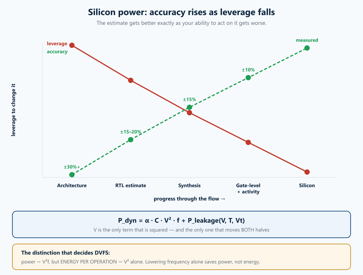
Accuracy. Poor — ±30% or worse. Leverage: total. Architectural choices dominate everything downstream, and they are all made here: how many cores, how much on-chip memory, how much data movement, what voltage and frequency the design targets.
The single most useful fact to carry into this step is the cost of moving data against the cost of computing on it. Order-of-magnitude, on a modern node:
| Operation | Energy |
|---|---|
| 32-bit integer add | ~0.03 pJ |
| 32-bit float multiply | ~0.4 pJ |
| 8 KB SRAM read | ~5 pJ |
| DRAM access | ~500 pJ |
A DRAM access costs roughly four orders of magnitude more than an add. Data movement, not arithmetic, is what an architecture spends its power on — which is why accelerator design is mostly memory-hierarchy design, and why “add more MACs” is rarely the answer to an efficiency problem.
Tools. Virtual platforms and architectural models — Synopsys Platform Architect, Cadence’s system design and verification flow — plus a great deal of in-house spreadsheet work, which is honest. See RTL power estimation for what this rung’s ±30% is actually made of.
Step 2 — RTL power estimation
What it does. Estimates power from RTL plus a simulation activity trace, before synthesis.
Accuracy. ±15–20% against final signoff, when the activity is representative. Leverage: high — this is the last point where an architectural or microarchitectural fix is cheap. Finding at RTL that a memory is being read every cycle when it needs to be read every fourth cycle is a day’s work; finding it after place-and-route is a schedule slip.
Tools. Ansys PowerArtist, Cadence Joules, Synopsys PrimePower RTL.
Step 3 — Power intent: UPF
What it does. Captures the power architecture as a machine-readable specification, separate from the RTL: which power domains exist, what voltage each runs at, which can be switched off, and what has to happen at every boundary between them.
What it must specify.Level shifters where a signal crosses a voltage boundary. Isolation cells so a powered-down domain’s floating outputs cannot corrupt a live domain. Retention registers for state that must survive a power-down. Power switches and their control and acknowledge sequencing. And the legal power state table — which combinations of domain states are allowed to exist.
Why it is a step and not a detail. Power intent is a specification that has to be verified against, and the failure mode is nasty: a missing isolation cell produces a design that simulates correctly in RTL (where there is no such thing as “powered down”) and fails in silicon when a floating input propagates X into a live domain. Power-aware simulation — simulation that actually honours the UPF — is what catches it, and it is not the default.
Formats.UPF (IEEE 1801) is the standard; CPF is the older Cadence-originated alternative.
Tools. Every flow reads UPF. The part that matters is low-power verification — proving the isolation, level-shifting and retention match the state table — with Synopsys VC LP, Cadence Conformal Low Power, or Siemens Questa power-aware simulation. This has to be a formal check: a missing isolation cell does not fail an ordinary simulation, it fails in silicon.
Step 4 — Synthesis with power optimisation
What it does. Implements the RTL, applying the power techniques automatically where the constraints allow.
Clock gating is the highest-value automatic optimisation. The clock tree is typically 30–40% of dynamic power, and it toggles by definition — so switching it off where it is not needed is pure saving:
| Clock share of dynamic | Fraction gated | Saving as % of dynamic |
|---|---|---|
| 30% | 50% | 15% |
| 30% | 70% | 21% |
| 40% | 70% | 28% |
| 40% | 90% | 36% |
Multi-Vt optimisation assigns high-Vt (slow, low-leakage) cells everywhere timing permits and spends low-Vt cells only on critical paths. The leverage is large and it is the main reason leakage is manageable at all.
Tools. Synopsys Design Compiler / Fusion Compiler, Cadence Genus.
Step 5 — Gate-level power with real activity
What it does. Annotates the placed-and-routed netlist with switching activity and computes power per instance.
This is where the activity problem bites. Two approaches, and the gap between them is the uncertainty in the whole flow:
- Vector-driven. Feed a real simulation trace — VCD or FSDB for full waveforms, SAIF for aggregated toggle statistics. Accurate for that workload. The catch: the peak power workload is rarely the functional test you happen to have, and a full-chip VCD for a realistic window is enormous.
- Vectorless. Propagate statistical activity from primary inputs. Covers everything, and is only as good as its assumptions — it will happily report a number for a state the design can never enter.
What α actually means, since it is the term people hand-wave:
| α | Toggles per second at 2 GHz |
|---|---|
| 0.01 | 20 M |
| 0.05 | 100 M |
| 0.10 | 200 M |
| 0.20 | 400 M |
Typical logic sits in the 0.05–0.15 range. A clock is α = 1 by definition. If a tool reports average logic activity near 0.5, the stimulus is wrong, not the design.
Goal. Two numbers, not one: average power (for thermal and battery) and peak power (for the PDN and the voltage regulator). They come from different workloads and are sized by different constraints.
Tools. Synopsys PrimePower, Cadence Joules / Voltus, Ansys PowerArtist.
Step 6 — IR drop and electromigration signoff
What it does. Takes the per-instance power from step 5 and checks the grid can deliver it — static IR, dynamic voltage drop, and EM on the power network.
This is the hand-off to part two, run on-die: the physics is identical, the tools are RedHawk-SC / Totem and Voltus, and the analysis is only as good as the activity that fed it.
The coupling that surprises people. IR drop is not just a power problem — it is a timing problem, because a cell at reduced supply is a slower cell:
| IR drop | Delay penalty |
|---|---|
| 1% | +1.1% |
| 3% | +3.4% |
| 5% | +5.9% |
| 10% | +12.9% |
A 5% droop costs roughly 6% of timing. That is why IR-drop results feed back into static timing as a voltage derate, and why signing off timing at nominal voltage while the grid droops 5% is a way to fail silicon.
Tools. Ansys RedHawk-SC, Cadence Voltus, Siemens mPower — the same three that do the dynamic analysis in the next step, because static and dynamic are modes of one tool rather than separate products.
Step 7 — Dynamic voltage drop and on-die decoupling
What it does. Checks the instantaneous droop from switching activity, and sizes the on-die decoupling capacitance that absorbs it.
Why on-die decap is a real budget decision. It costs area and it leaks. But as part two established, above roughly a gigahertz the package inductance isolates the die from every capacitor on the board — so on-die decap is the only thing supplying the fastest transients. The trade is explicit: area and leakage against droop.
Tools. Ansys RedHawk-SC and Cadence Voltus in dynamic mode, driven by per-cycle activity rather than an average — an averaged vector cannot produce a droop number, because the information about when has already been discarded.
Step 8 — Thermal
What it does. Turns the power map into a temperature map, and feeds the temperature back into leakage and timing.
Why it closes the loop. Everything above assumed a temperature. Thermal analysis tells you whether that assumption was right, and because leakage is exponential in temperature, being wrong is not a small error.
Tools. Ansys Icepak and RedHawk-SC Electrothermal, Cadence Celsius.
Step 9 — Silicon measurement
What it does. Measures what the part actually draws, per rail, across workloads and temperature.
How. Rail instrumentation on the bench, on-die power monitors and thermal diodes, and per-workload characterisation. The output is the correction factor for the next design’s estimates — the same calibration argument as silicon correlation in part four.
Tools. Not EDA. Bench instruments — current probes and shunts on each rail, a thermal camera, and whatever on-die power and temperature monitors were designed in. The last of those is the one to insist on at floorplan time: a chip with no on-die monitors can only be measured at the package pins, which averages away exactly the per-block detail the correlation needs.
3. The techniques, and what each is worth
| Technique | Attacks | Typical leverage | Cost |
|---|---|---|---|
| Clock gating | Dynamic | 15–35% of dynamic | Almost none; largely automatic |
| Multi-Vt | Leakage | Large | Timing pressure on critical paths |
| Power gating | Leakage | Near-total for the off domain | Area, wake latency, inrush, retention |
| DVFS | Both | Very large | Control complexity, regulator support |
| Operand isolation | Dynamic | Block-specific | Small area |
| Memory banking / clock gating | Dynamic | Large in memory-heavy designs | Architecture work |
DVFS deserves its own arithmetic, because it is the most misunderstood. Power goes as , but energy per operation goes as V² alone — it does not depend on frequency:
| Operating point | Power | Energy/op | Throughput |
|---|---|---|---|
| 0.90 V, 2.0 GHz | ×1.000 | ×1.000 | ×1.00 |
| 0.80 V, 1.6 GHz | ×0.632 | ×0.790 | ×0.80 |
| 0.70 V, 1.2 GHz | ×0.363 | ×0.605 | ×0.60 |
| 0.60 V, 0.8 GHz | ×0.178 | ×0.444 | ×0.40 |
Read the second and third columns together. Lowering frequency alone saves power but not energy — the work still costs the same, it just takes longer, and for a fixed workload you finish later having used the same joules. Only lowering voltage reduces the energy per operation. This is why “race to idle” can beat “run slowly” whenever a deep low-power state exists, and why DVFS is only worth its complexity if the voltage moves with the frequency.
Power gating’s hidden cost is inrush. Switching a domain back on recharges all of its decoupling capacitance at once, and that current step is exactly the di/dt event part two warned about. Well-designed power switches ramp in stages — a weak switch first, the strong one after — for precisely this reason.
4. The tools, by step
| Step | Tool | Note |
|---|---|---|
| Architectural budget | Platform Architect, TLM models, spreadsheets | ±30%, and the most leverage you will ever have |
| RTL power estimation | PowerArtist, Joules, PrimePower RTL | ±18% with real activity; the diagnostics matter more than the total |
| Power intent (UPF) | Written by hand, read by everything | IEEE 1801; CPF in older flows |
| Low-power verification | VC LP, Conformal Low Power, Questa power-aware | Formal — a missing isolation cell does not fail simulation |
| Synthesis with power opt | Design Compiler / Fusion Compiler, Genus | Clock gating, multi-Vt, operand isolation |
| Gate-level power | PrimePower, Joules, Voltus, PowerArtist | ±13% post-synthesis, ±8% post-layout with SPEF |
| Static IR and EM | RedHawk-SC, Voltus, mPower | Feeds back into STA as a voltage derate |
| Dynamic voltage drop | RedHawk-SC, Voltus (dynamic mode) | Needs per-cycle activity; an average cannot produce a droop |
| Thermal | Icepak, RedHawk-SC Electrothermal, Celsius | Leakage and temperature are a feedback loop |
| Silicon measurement | Rail shunts, thermal camera, on-die monitors | Not EDA; the output is next design’s correction factor |
Two things that table makes visible. The same three engines — RedHawk-SC, Voltus, mPower — do static IR, dynamic droop and electromigration, because they are modes of one analysis rather than separate products; the flow decision is usually which vendor stack, not which tool. And the rows divide cleanly into estimation and signoff: everything down to gate-level power is a number you act on, and everything below it is a gate you pass. The accuracy ladder explains why those two halves behave so differently.
5. Best practices
- Budget top-down early and track it. The architecture decides the power; everything after is a percentage.
- Count data movement, not operations. A DRAM access is ~10⁴ × an add.
- Estimate at RTL, where a fix is still cheap.
- Write the UPF as a specification, and verify against it. Power-aware simulation is not the default and a missing isolation cell will not show up without it.
- Report average and peak separately. Thermal is sized by one, the PDN by the other.
- Say where the activity came from. A power number without its stimulus is not a number.
- Sanity-check α. Logic in the 0.05–0.15 range; anything near 0.5 means broken stimulus.
- Sign off power at the hot corner, iterated with thermal — and do not extrapolate the leakage doubling rule across a 100 °C span.
- Feed IR drop back into timing as a derate. A 5% droop is ~6% of timing.
- Stage the power-switch turn-on so wake-up inrush does not collapse the rail.
The pitfalls that cost the most time
- A power number quoted without the workload that produced it.
- Vectorless activity reported as though it were measured.
- Signing off timing at nominal voltage while the grid droops.
- Extrapolating “leakage doubles every 10 °C” across the full temperature range.
- Forgetting that a powered-down domain’s outputs float unless isolated.
- Assuming clock gating happened because the tool was asked to do it — check the reported gating efficiency.
- Sizing the regulator for average power and discovering peak on the bench.
- Treating on-die decap as free area.
Where we fit
Our primary work is board-level — schematic, layout, stackup, and signal- and power-integrity analysis in Cadence Allegro, Altium, Ansys SIwave and Siemens HyperLynx — plus the FMEDA and FMEA evidence where a programme carries a functional-safety requirement. Silicon power matters to that work at the boundary: the chip’s peak current and di/dt profile are the inputs that size the board’s PDN and its regulator, and a chip-side number that is wrong in either direction shows up as a board that droops or a bill of materials that is needlessly expensive.
If you have a power budget that does not close, or a rail specified from a number nobody can source, that is the conversation we like having.
Glossary
Activity factor (α) — The fraction of clock cycles on which a node toggles, and the one term in that cannot be read off the netlist. Random logic runs 0.05–0.15; a clock is 1 by definition, which is why clock trees dominate dynamic power. Getting α wrong is the single largest source of error in a power estimate, and it is why the stimulus matters more than the tool.
CPF — Common Power Format, the older Cadence-originated alternative to UPF. Still found in established flows; new work uses UPF, and mixed-format projects pay for the translation.
DVFS — Dynamic Voltage and Frequency Scaling. Because dynamic power goes as and the achievable itself rises with , dropping voltage buys back power roughly cubically — which is why it is the highest-leverage knob in the list, and why it drags in level shifters, characterisation at extra corners, and a controller that must never outrun the regulator.
Dynamic voltage drop (DvD) — Instantaneous supply droop caused by switching, as opposed to static IR. It is local and momentary, so a rail can look healthy on average and still brown out in one block on a simultaneous clock edge — see power integrity.
Isolation cell — Clamps a powered-down domain’s outputs to a defined level so its floating outputs cannot corrupt a live domain. Omitting one does not fail simulation with a default netlist — it fails in silicon, which is why power intent is verified formally rather than by eye.
Leakage — Current drawn with nothing switching: subthreshold conduction, gate tunnelling and junction leakage. Exponential in temperature and in threshold voltage, so it is a corner problem (hot, low-Vt, fast process) rather than a nominal one, and it is the reason power gating exists at all.
Level shifter — Translates a signal crossing between two supply voltages. Needed in both directions and they are not the same cell; a low-to-high shifter that is fed from a domain which can also power down needs isolation as well, which is where the cell count starts surprising people.
Multi-Vt — Mixing threshold-voltage flavours: low-Vt where the path is critical and the leakage is worth it, high-Vt everywhere else. The standard first move in leakage reduction because synthesis can do it automatically, and the usual outcome is that a few per cent of cells are low-Vt and carry most of the leakage.
Operand isolation — Holding a datapath’s inputs stable when its result will not be used, so the arithmetic does not toggle for nothing. Cheap, effective on wide multipliers and unused execution units, and applied automatically by modern synthesis where the enable is easy to prove.
Power gating — Switching a domain’s supply off entirely, removing its leakage rather than reducing it. Costs area for the switch, wake-up latency, in-rush current that the PDN must survive, and a retention strategy for whatever state must survive — so it pays on blocks that are idle for long stretches, not on ones that are idle briefly.
Power state table — The enumeration of legal combinations of domain power states. It is the specification that isolation, level-shifting and retention are checked against; an incomplete table means the checks pass while a real state goes unverified.
Retention register — A flop that keeps its value through a power-down, using a shadow latch on an always-on supply. Bigger and leakier than a plain flop, so retaining everything defeats the purpose — the design decision is which state is cheaper to keep than to recompute.
SAIF / VCD / FSDB — Activity formats. VCD and FSDB are full waveform dumps (accurate, enormous); SAIF carries aggregated toggle counts and durations (small, sufficient for average power). Choose by what you are computing: peak and droop need waveforms, average power does not.
Short-circuit power — Power burned while pull-up and pull-down conduct simultaneously during a transition. Small on a well-designed gate with a fast input slew, and it grows quickly as slews degrade — so it is one of the ways a marginal-slew net costs more than its timing number suggests.
Thermal runaway — Leakage raising temperature, raising leakage, with no stable operating point. The reason leakage must be evaluated at the hot corner together with the package thermal resistance, and a real risk in high-density, high-Vdd, poorly-cooled designs.
UPF — Unified Power Format, IEEE 1801: the standard way to state power intent — domains, supplies, state tables, isolation and retention strategies — separately from the RTL. Keeping it out of the RTL is what lets the same RTL be synthesised with different power architectures.
Vectorless estimation — Propagating activity statistically from a few assumed input toggle rates instead of from a simulation. Useful before RTL simulation exists, and it cannot know that your bus is idle 90% of the time or that two blocks never run together. Treat it as a sanity check, never as a number to sign off.
Further reading — reference books
Book links below are Amazon affiliate links: if you buy through one we earn a small commission at no extra cost to you. It does not influence what is recommended — the same books were on this list before the links were.
- Rabaey, Chandrakasan & Nikolić, Digital Integrated Circuits: A Design Perspective — the power chapters are the standard treatment.
- Weste & Harris, CMOS VLSI Design: A Circuits and Systems Perspective.
- Jan Rabaey, Low Power Design Essentials.
- Michael Keating et al., Low Power Methodology Manual: For System-on-Chip Design.
- Taur & Ning, Fundamentals of Modern VLSI Devices — for where leakage actually comes from.
- IEEE Std 1801 (UPF), the power-intent standard itself.
Have a power budget that will not close, or a rail sized from a number nobody can source? That’s what we do. Reach us at circuit-design.space.
circuit-design.space · +1-971-357-1400 · anovickis@circuit-design.space