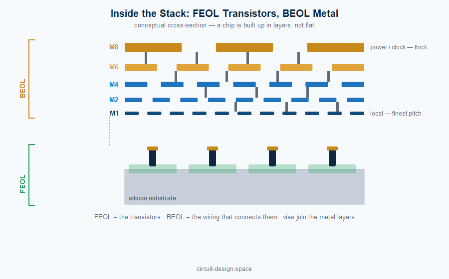
What a semiconductor process node actually is, how transistors evolved from planar to FinFET to gate-all-around, the FEOL/BEOL layer stack, why design rules and DRC exist, and how process geometry shapes every chip design decision.
Posts by alex.novickis@gmail.com

From Concept to Tapeout: The ASIC Design Flow, Step by Step
A practical walkthrough of the ASIC design flow from concept to tapeout — every step broken out with why it exists, its goal, how it works, how long it takes, and the Synopsys, Cadence, Siemens EDA and Ansys tools used, plus the ISO 26262 ASIL B/D safety overlay, analog vs digital, MPW, and a glossary.
Mapping ML Workloads to Silicon: Why Inference Is a Memory Problem
A new open-access paper: why batch-1 LLM inference is bound by memory bandwidth, not FLOPS — and a memory-first accelerator design (FMCT) with an inline KV-cache compression engine.