First in a five-part series on the physics of getting signals and power across a real system. This part covers signal integrity — the channel from die to die. Part two covers power integrity, from DC drop to di/dt. Part three covers RF and microwave design. Parts four and five move inside the die: on-die signal integrity and silicon power usage.
Signal integrity answers one question: does the receiver recover the bit the transmitter sent, with margin, over temperature, process and time? Everything below — every formula, every solver, every measurement — exists to answer that question before the board is built, and to explain the answer when the board is on the bench and the link will not train.
The hard part is rarely the physics. The physics has been settled since Heaviside. The hard part is choosing the cheapest model that still tells the truth, because the honest 3D answer to every question would take a week per structure and nobody has a week per structure. That judgement — which solver, at which fidelity, for which piece of the channel — is most of the job, so it is most of this article.
1. When a wire stops being a wire
A copper trace behaves as a lumped connection when the signal takes far less time to traverse it than to change state. Once that stops being true, the trace is a transmission line and you are in the business of managing reflections.
The usual working threshold is the electrical length against the signal’s rise time. A trace needs transmission-line treatment when its one-way delay exceeds roughly one sixth of the rise time — some houses use one tenth, some one half; the number is a convention, the gradient is real.
The companion rule is Johnson’s knee frequency — the frequency above which a digital edge’s spectrum has essentially no energy, and therefore the frequency your model has to be good up to:
| Rise time | Comment | |
|---|---|---|
| 1 ns | 0.5 GHz | slow logic; lumped models survive |
| 100 ps | 5 GHz | a 2D solver and a good line simulator will do |
| 35 ps | 14.3 GHz | 56G PAM4 territory; 3D for every discontinuity |
| 20 ps | 25 GHz | everything is a resonator |
Note what this says: rise time, not clock rate, sets the bandwidth you must model. A 100 MHz clock with a 100 ps edge is a 5 GHz problem. Engineers who model to the clock frequency and not to the knee build boards that fail for reasons their simulation could not see.
Propagation delay, computed rather than remembered:
| Medium | ε_r | Velocity | Delay |
|---|---|---|---|
| Vacuum / air | 1.0 | 299.8 mm/ns | 84.7 ps/inch |
| Low-loss laminate | 3.0 | 173.1 mm/ns | 146.7 ps/inch |
| Mid-loss laminate | 3.6 | 158.0 mm/ns | 160.8 ps/inch |
| FR-4 stripline | 4.3 | 144.6 mm/ns | 175.7 ps/inch |
Microstrip is faster than stripline on the same laminate because part of its field is in air, so its effective ε_r is lower than the bulk value. That is also why microstrip and stripline on the same board do not match in delay — a fact that ends up mattering for skew budgets on parallel buses and for differential pairs that change layer.
2. The transmission line, in the four numbers that matter
A uniform line is fully described per unit length by R, L, G, C — the telegrapher’s parameters. Everything an SI engineer quotes is derived from them.
The lossless approximation is the one to keep in your head, because it explains every impedance problem you will ever debug. Impedance is wrong when either the inductance or the capacitance per unit length is wrong. A trace over a gap in the reference plane has too much L. A pad, a via antipad that is too small, a connector’s contact region — too much C. That is the whole diagnosis.
Loss: three mechanisms, three different frequency slopes
Conductor loss comes from finite copper conductivity, concentrated by the skin effect into a thin surface layer:
| Frequency | Skin depth in copper | Surface resistance |
|---|---|---|
| 1 MHz | 65.2 µm | 0.26 mΩ/sq |
| 100 MHz | 6.52 µm | 2.58 mΩ/sq |
| 1 GHz | 2.06 µm | 8.14 mΩ/sq |
| 10 GHz | 0.652 µm | 25.8 mΩ/sq |
| 28 GHz | 0.390 µm | 43.1 mΩ/sq |
Two consequences fall out immediately. First, conductor loss rises as . Second — and this is the one that surprises people — at 10 GHz the current lives in the outer 0.65 µm of the copper, which is smaller than the tooth profile of the foil. Copper roughness is therefore not a cosmetic parameter; it is a first-order loss term. The Hammerstad correction (a bounded multiplier, saturating near 2×) is adequate to about 5 GHz; above that the Huray “snowball” model, which treats the roughness as a packed set of spheres, is what correlates. Getting roughness wrong is the single most common reason a simulated insertion loss curve sits optimistically below the measured one.
Dielectric loss comes from the laminate’s loss tangent and rises linearly with frequency:
| Laminate class | tanδ | Loss at 10 GHz | At 28 GHz | |
|---|---|---|---|---|
| Mid-loss | 3.6 | 0.008 | 0.138 dB/cm (0.35 dB/in) | — |
| Low-loss | 3.0 | 0.002 | 0.032 dB/cm (0.080 dB/in) | — |
| Ultra-low-loss | 3.2 | 0.0035 | — | 0.160 dB/cm (0.41 dB/in) |
Because conductor loss goes as and dielectric loss as , there is a crossover: below it copper dominates, above it the laminate dominates. On typical stackups that crossover lands somewhere in the low-GHz decade, which is exactly why the 10–25 Gbps generation of designs was the one that forced the industry onto low-loss materials.
Causality and dispersion. is not constant. A model that holds fixed while tanδ is non-zero is non-causal — it will produce a step response that starts before the step, and a time-domain simulation will show it. The Djordjevic–Sarkar (wideband Debye) model ties the real and imaginary parts together so the material behaves causally across the band. Use it. Any serious 2D/3D tool offers it; the failure mode of not using it is a model that looks fine in the frequency domain and produces nonsense in the time domain.
3. The five mechanisms that close an eye
Every SI failure is one of these, or a combination:
Reflections. An impedance discontinuity returns energy. Amplitude is the reflection coefficient, and it is worth memorising how forgiving — or not — the numbers are:
, ,
on a 50 Ω line Return loss VSWR 55 Ω (10% high) 0.048 26.4 dB 1.10 60 Ω (20% high) 0.091 20.8 dB 1.20 75 Ω 0.200 14.0 dB 1.50 100 Ω 0.333 9.5 dB 2.00 A ±10% impedance tolerance — the standard fab spec — is a 26 dB return loss floor before you have designed anything. That is the budget you start with, not the budget you end with.
Loss and ISI. Attenuation is frequency-dependent, so a pulse spreads into its neighbours. This is what equalization exists to undo, and it is the mechanism that sets how long a channel can be.
Crosstalk. Mutual inductance and capacitance couple aggressor to victim. NEXT (near-end) appears at the driver end and saturates with coupled length; FEXT (far-end) accumulates with coupled length and is proportional to the difference between inductive and capacitive coupling — which is why FEXT is much worse in microstrip (inhomogeneous dielectric) than in stripline (homogeneous), where the two coupling terms nearly cancel. If you take one layout rule from this article: run long parallel differential pairs in stripline.
Mode conversion. A differential pair with intra-pair skew, asymmetric routing, or an asymmetric via transition converts differential energy to common mode () and back. Common mode is what radiates, what couples into neighbouring systems, and what fails EMC. Fibre-weave effects — the glass bundles of the laminate weave sitting under one leg of a pair and not the other — are a leading cause on long, fast links, and are the reason for zig-zag routing and spread-glass materials.
Resonances. Anything unterminated is a resonator. The classic is the via stub: the unused barrel below the exit layer forms a quarter-wave open stub that puts a deep null in the insertion loss.
Stub length (ε_r = 4) First null 2.0 mm 18.7 GHz 1.5 mm 25.0 GHz 1.0 mm 37.5 GHz 0.5 mm 75.0 GHz A 1.5 mm stub — a signal entering on layer 2 of a 1.6 mm board — puts a null at 25 GHz, directly on top of the 28 GHz Nyquist of a 112G PAM4 lane. This is why back-drilling exists, and why “how deep is the drill and what is the tolerance” is a real design parameter and not a fab detail.
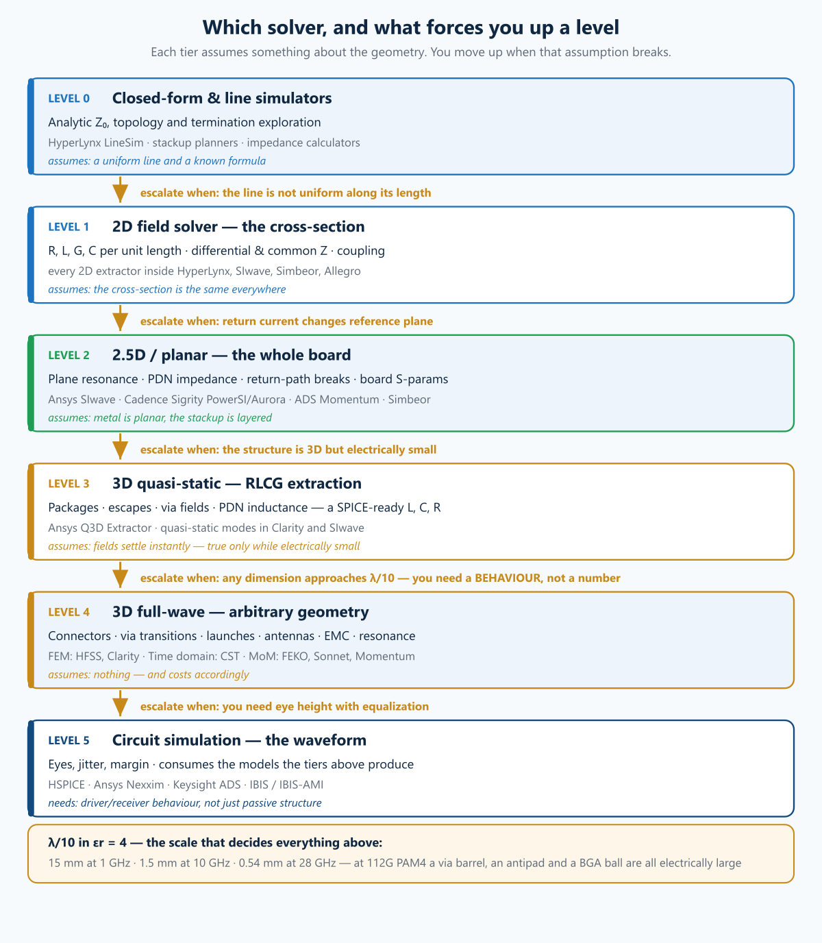
4. The solver taxonomy — the actual decision
Here is the hierarchy, cheapest to most expensive, with the question each level can and cannot answer.
Level 0 — Closed-form and line simulators
What it is. Analytic impedance formulas (Wheeler, Hammerstad–Jensen, IPC-2141) and schematic-level topology exploration with ideal or lightly-modelled T-line elements. Tools: HyperLynx LineSim, the stackup/impedance planners inside Allegro and Altium, Simbeor’s impedance calculators.
Answers. Stackup selection. Nominal trace widths for a target impedance. Termination topology — series, parallel, Thévenin, is a T-branch survivable, where should the stub go. First-order timing and reflection behaviour on a bus.
Cannot answer. Anything involving a discontinuity’s actual geometry: vias, connector launches, plane splits, package escapes. Anything above a few GHz with confidence.
Use it at the front of the project, on day one, before layout exists. It is the only tool in the list that is fast enough to explore twenty topologies in an afternoon, and that exploration is worth more than any single accurate simulation later.
Level 1 — 2D field solvers (the cross-section)
What it is. A numerical solution of the static or quasi-static field over the uniform cross-section of a line, producing the R, L, G, C matrices per unit length — and, for coupled lines, the full coupling matrices.
Answers. Accurate characteristic impedance, differential and common-mode impedance, odd and even mode velocities, per-unit-length crosstalk coefficients, loss including skin effect and (with a roughness model) foil texture.
Cannot answer. Anything that varies along the length. A 2D solver assumes the cross-section is the same everywhere and the propagation is a single TEM-like mode.
Use it for every routed trace segment, always. This is the workhorse. Ninety percent of the copper on any board is uniform, and 2D solves it in milliseconds to an accuracy that a 3D solver will not meaningfully improve. Feeding 3D solvers with long uniform sections is the most common way engineers waste compute.
Level 2 — 2.5D / planar solvers
What it is. A method-of-moments or hybrid formulation that treats arbitrary geometry in the plane but assumes a layered stackup in the vertical direction. Currents flow in horizontal metal, vias connect layers as short vertical elements. Tools: Ansys SIwave, Cadence Sigrity PowerSI/Aurora, Keysight ADS Momentum, Simbeor.
Answers. Full-board behaviour: plane resonances, power-ground cavity modes, board-level crosstalk between arbitrary nets, return-path discontinuities across splits, S-parameters of a whole PCB with hundreds of ports. This is the only class of tool that can swallow an entire board and give you an answer today.
Cannot answer. Fine 3D structure: the internal geometry of a connector, a bond wire arc, a ball-grid array’s true 3D field, a radiating structure, anything where the vertical dimension is comparable to a wavelength.
Use it for board-scale questions and for every PDN question (see part two). For SI it is the right tool for “does this net see a return-path problem anywhere on this 14-layer board”, which is a question no 3D solver can be pointed at.
Level 3 — 3D quasi-static extraction (the rung people skip)
What it is. A full 3D solution of the static and magnetostatic fields over arbitrary geometry, producing an RLCG matrix — but without solving the wave equation. Tools: Ansys Q3D Extractor, the quasi-static modes inside Clarity and SIwave.
Answers. Accurate partial inductance, loop inductance, capacitance and DC/AC resistance of a genuinely 3D structure: a package, a BGA escape, a connector at moderate frequency, a bus bar, a via field, the current path from a capacitor pad to a plane pair. It produces a lumped or distributed equivalent circuit you can drop straight into SPICE.
Cannot answer. Anything where the structure is a meaningful fraction of a wavelength — resonance, radiation, propagation delay, mode conversion. It assumes fields settle instantaneously, which is exactly the assumption that fails once dimensions approach λ/10.
Use it when the structure is 3D but electrically small. That combination is extremely common and it is where the most compute gets wasted: a full-wave solve of a package escape at 200 MHz gives you the same L and C that a quasi-static solve gives you in a fraction of the time, with a convergence story that is easier to defend. This is also the right tool for most PDN inductance questions — mounting inductance, spreading inductance, package inductance — because those are inductance extractions, not wave problems.
The rule of thumb: is the answer I want a number (L, C, R), or a behaviour (resonance, radiation, delay)? Numbers are quasi-static. Behaviours are full-wave.
Level 4 — 3D full-wave solvers
What it is. Maxwell’s equations solved over an arbitrary 3D volume, with no assumption about geometry or mode structure. Three main numerical families, and the choice between them is not arbitrary:
FEM — finite element method, frequency domain. Tools: Ansys HFSS, Cadence Clarity. Tetrahedral mesh, adaptively refined until the S-parameters stop moving. Strengths: conforming mesh handles curved and irregular geometry beautifully; adaptive refinement gives a convergence metric you can defend; excellent for resonant and highly-detailed structures. Weakness: one solve per frequency (mitigated by interpolating sweeps), and memory grows fast with volume.
FIT / FDTD — time domain. Tools: CST Studio Suite (finite integration technique), various FDTD codes. One transient run yields the whole band via FFT. Strengths: broadband in a single solve, scales well to electrically large problems, natural for transient and EMC work. Weakness: staircase meshing of curved geometry (mitigated by conformal/PBA schemes), and structures with high Q take a long time to ring down.
MoM — method of moments, integral equation. Tools: CST’s I-solver, FEKO, ADS Momentum in its 3D modes. Only meshes the conductors, not the surrounding air, so it is extremely efficient for radiating structures and electrically large metallic bodies. Weakness: inhomogeneous volumetric dielectrics are awkward.
The practical rule: FEM for connectors, packages, via transitions and anything with intricate 3D detail and a defined port set. Time domain for electrically large structures, broadband transients and EMC/enclosure work. MoM for antennas and large conductive bodies. Where two would work, use the one your team can validate against measurement, because a solver you cannot correlate is a solver you cannot trust.
Level 5 — Circuit simulation
Field solvers produce models. Circuit simulators consume them and produce waveforms.
- SPICE / HSPICE — the reference for transient accuracy, W-element transmission lines, and anything involving real transistor-level driver behaviour. Slow, exact, the arbiter when two faster tools disagree.
- Ansys Nexxim — the circuit engine paired with HFSS/SIwave in the Ansys flow; handles large S-parameter sets, convolution with measured/simulated channels, and transient co-simulation with field-solved blocks.
- Keysight ADS — the RF/SI hybrid: harmonic balance, envelope, channel simulation, and a strong statistical eye engine.
- IBIS and IBIS-AMI — behavioural driver/receiver models. Plain IBIS gives you the analog buffer (V/I curves, ramp rates) for reflection and timing work. IBIS-AMI adds the vendor’s equalization algorithms — CTLE, FFE, DFE, CDR — as compiled code, which is the only legitimate way to simulate a modern SerDes link, because the silicon’s adaptation is the thing that decides whether the link closes.
The escalation triggers
You move up a level when one of these becomes true:
| Trigger | Move to |
|---|---|
| The structure is not uniform along its length | 2D → 2.5D or 3D |
| Return current has to change reference planes | at least 2.5D |
| Vertical geometry is comparable to horizontal | 2.5D → 3D |
| The structure is 3D but electrically small, and you want L / C / R | 3D quasi-static (Q3D) |
| Any dimension approaches λ/10 in the dielectric | 3D full-wave |
| You need resonance, delay or mode conversion, not just L and C | 3D full-wave |
| The structure radiates, or you care about EMC | 3D (time domain or MoM) |
| You need the real behaviour of a connector or package at speed | 3D FEM |
| You need eye height/width with equalization | circuit + IBIS-AMI |
For scale: λ/10 in = 4 is 15 mm at 1 GHz, 1.5 mm at 10 GHz, and 0.54 mm at 28 GHz. At 112G PAM4 rates, a via barrel, an antipad, and a BGA ball are all electrically significant structures. That is the whole reason 3D extraction became mandatory rather than optional.
5. The tools, and what each is actually for
| Tool | Class | Where it earns its licence |
|---|---|---|
| HyperLynx LineSim / BoardSim | Line sim + 2D/2.5D | Fast pre- and post-layout batch DRC-style SI sweeps across a whole board; the “did anything get worse” regression tool |
| Ansys SIwave | 2.5D planar | Board-scale S-parameters, DC IR, plane resonance, PDN impedance; the SI/PI workhorse for real boards |
| Ansys Q3D Extractor | 3D quasi-static | RLCG of electrically-small 3D structures: packages, escapes, via fields, PDN inductance — a SPICE-ready model without paying for full-wave |
| Ansys HFSS | 3D FEM | Connectors, packages, via transitions, launches, anything where geometry is the answer |
| Cadence Clarity | 3D FEM | Same class as HFSS, distributed-solve architecture; strong when it sits natively beside Allegro/Sigrity data |
| Cadence Sigrity (PowerSI, PowerDC, Aurora, Topology Explorer) | 2.5D + flow | Board/package extraction and PI inside the Cadence ecosystem; Topology Explorer for pre-layout what-ifs |
| CST Studio Suite | 3D time domain / multi-method | Broadband single-run extraction, electrically large structures, EMC, enclosures, antennas |
| Simbeor | 2D/3D hybrid + material ID | Best-in-class at material and roughness identification from measured data — the step that makes every other model correlate |
| Keysight ADS | Circuit + EM | RF and SI in one environment; harmonic balance, channel sim, statistical eyes |
| Ansys Nexxim | Circuit | Transient/convolution engine behind the Ansys SI flow, large-S-parameter handling |
| HSPICE | Circuit | The reference transient simulator; W-element lines; the arbiter |
| Keysight PLTS | Measurement post-processing | Turns raw VNA/TDR data into usable models: de-embedding, mixed-mode conversion, causality/passivity enforcement, measurement-to-simulation overlay |
On PLTS specifically, because it is often misunderstood: it is not a solver. It is the bridge between the bench and the simulator. It takes measured S-parameters, applies fixture removal, converts single-ended to mixed-mode, checks and enforces passivity and causality, and lets you overlay measurement against simulation in both domains. That overlay is where you find out whether your model is right — and a model you have never overlaid on a measurement is a hypothesis, not a model.
6. Connector modeling
Connectors are the hardest passive structures in a channel, and they are where the most simulation effort goes for the least visible reward. Three reasons:
- They are irreducibly 3D. Contact beams, compliant pins, ground shields, the housing dielectric, the transition from a round pin to a flat pad — none of it is planar, none of it is uniform, and all of it is the same order of size as the wavelengths in question.
- They are the impedance discontinuity by construction. A connector’s job is mechanical; its electrical behaviour is a compromise with that job. Every mating interface is a place where the local L/C ratio departs from the line.
- The launch dominates. More connector performance is lost in the footprint — the antipad, the via, the escape routing, the ground-via placement around the signal — than in the connector body itself. A superb connector on a careless footprint measures worse than a mediocre connector on a good one.
How the model gets built
Geometry. Start from the mechanical CAD, then simplify deliberately. Fillets, knurls, retention features and plating layers that are far from the current path cost mesh and buy nothing. Features in the contact region and the ground return path buy everything. Knowing which is which is the skill.
Materials. Bulk conductivity of the contact alloy — not copper, usually a phosphor bronze or beryllium copper with a meaningfully lower conductivity. Plating stack matters where it is thicker than the skin depth: at 10 GHz, δ is 0.65 µm, so a 1.3 µm gold flash is more than two skin depths and the field never sees the substrate. Nickel underplate is the trap — it is ferromagnetic and lossy, and a nickel layer in the current path shows up as excess insertion loss that no amount of geometry tuning will explain.
Ports and de-embedding. This is where most connector models go wrong. A wave port must be placed on a uniform section of line, sized to enclose the field but not so large that it supports higher-order modes, and referenced to the correct conductor. If the port sits in a region that is still transitioning, the solver dutifully reports the impedance of a structure that does not exist in the real assembly. Extend the geometry with uniform line, port on that, and de-embed back to the reference plane you actually mean.
Meshing and convergence. Adaptive refinement in FEM should be driven to a ΔS criterion tight enough that the last two passes agree to better than the effect you are trying to measure. If you are chasing a 0.2 dB difference between two footprint options, a 0.02 convergence target is not good enough. And always solve at a frequency high enough to seed the mesh for the top of your band — a mesh converged at 1 GHz is not a mesh at 40 GHz.
Symmetry. Symmetry planes (perfect E, perfect H) can cut the problem by 2× or 4×. They are also the fastest way to get a wrong answer, because a symmetry plane suppresses every mode that is antisymmetric about it — including, sometimes, the mode that is causing your problem. Use symmetry to speed up a characterised structure; never to explore an uncharacterised one.
What a delivered connector model must have. Broadband to at least 3× the Nyquist of the target rate; passive (no S-parameter magnitude above unity for a passive structure, at any frequency); causal; reciprocal ( = ); DC-extrapolated correctly; and with a clearly documented reference plane and port map. A Touchstone file without a stated reference plane is not a deliverable.
Correlation. The model is validated against a measured mated pair, on a fixture that has itself been de-embedded. The two curves will not lie on top of each other. The question is whether they diverge in a way you can explain — roughness, plating, a mechanical tolerance — or a way you cannot. Explaining the divergence is the deliverable; a suspiciously perfect match usually means the measurement and the simulation share an error.
7. Channel modeling: assembling the pieces
A serial link is a cascade: die → package → via/launch → PCB trace → connector → cable or backplane → connector → trace → package → die. Each block is characterised by whatever method suits it — 3D for the connectors and vias, 2D for the uniform trace, vendor models for the package — and the blocks are cascaded in S-parameters (via T-parameters, which multiply) or in a circuit simulator.
Where cascades go wrong:
- Reference-plane mismatch. Two blocks that both include the same half-inch of launch, or neither of them does. This is the single most common channel-modeling error, and it shows up as an impedance ripple no one can source.
- Port ordering and polarity. A silent, catastrophic error class. Differential pairs swapped, or single-ended ports assigned in a different order than the netlist assumes. Always sanity-check with a TDR of the assembled cascade: the impedance profile should narrate the physical journey.
- Insufficient bandwidth or resolution. A Touchstone file that stops at 20 GHz cannot be convolved to produce a 17.86 ps UI eye. Frequency spacing sets the time-domain window; too coarse and you get aliasing that looks like reflections.
- Non-passive, non-causal data. Measured data almost always violates both slightly. Enforce them (PLTS, or the enforcement in your circuit tool) before convolution, or the time-domain result will contain energy the structure never had.
Quality checks to run on every S-parameter file, every time:
- Passivity — the eigenvalues of are at every frequency.
- Reciprocity — for a passive structure.
- Causality — the Hilbert-transform relation between magnitude and phase holds.
- DC behaviour — extrapolation to 0 Hz is physical, not an artefact.
- No unexplained nulls — insertion loss is monotonic-ish; a null means a resonator.
De-embedding removes the test fixture. The methods, in increasing order of robustness and effort: short-open-load-thru (SOLT) calibration to the connector; TRL (thru-reflect-line) with fabricated standards on the same panel — the gold standard, and self-consistent because the standards share the fabrication error; 2x-thru / AFR per IEEE 370, which extracts the fixture from a symmetric thru and needs no extra standards. IEEE 370 also defines the quality metrics that make fixture removal auditable, and citing it is the easiest way to make a channel model reviewable by someone who did not build it.
Analysis, finally. Two schools:
- Time-domain / statistical eyes. Convolve the channel with a PRBS pattern and the driver/receiver AMI models, accumulate an eye, read height and width at a target BER. Realistic; slow; needs enough bits to reach the BER you care about (which is why bit-by-bit simulation to 1e-12 is impossible and statistical methods exist).
- COM — Channel Operating Margin, defined in IEEE 802.3. A single scalar, in dB, that rolls insertion loss, reflections, crosstalk and a reference equalizer into one number against a specified reference receiver. Its value is that it is specified: two parties can agree a channel passes without agreeing on their proprietary receivers. Its limit is the same: it is a reference receiver, not your receiver.
8. What changes on the chip side
The physics is identical; the scales, tools and dominant effects are not.
On-die interconnect is resistive in a way board copper never is. A minimum-width metal-1 wire is dominated by R, not L — the RC delay is the design constraint, and repeater insertion is the answer. Inductance only becomes relevant on wide, long, low-resistance upper-metal routes: clock spines, power straps, and the top-metal RF and SerDes routing.
Extraction is the equivalent of your 2D solver: StarRC, Quantus and their equivalents produce the parasitic netlist from the layout, using pattern-matched or field-solved rules. Signoff-grade extraction with a real field solver in the loop is reserved for the critical nets — clocks, high-speed I/O, sensitive analog — because doing it everywhere is prohibitive.
On-die EM structures — inductors, transformers, transmission lines in top metal, pads and ESD structures — get the same 3D treatment as board structures, from the same solvers (HFSS, EMX, Momentum), with the added complication of a lossy, conductive silicon substrate that couples everything to everything.
The chip-side tool map
The same “cheapest model that still tells the truth” logic applies on-die, with a different cast. Read this table the same way as the board one — the middle column is the trigger.
| Question on the chip | Reach for | Why that tier |
|---|---|---|
| Parasitics of ordinary routed nets | StarRC, Quantus, Calibre PEX | Pattern-matched / rule-based extraction; fast enough to run over a whole block |
| Signoff parasitics on critical nets (clock, high-speed I/O, sensitive analog) | the same tools in field-solver mode | Rule-based extraction is calibrated, not solved; the critical few justify the real solve |
| On-die inductors, transformers, top-metal T-lines, pads, ESD | EMX, HFSS, ADS Momentum | Genuine 3D EM over a lossy conductive substrate — nothing about it is quasi-TEM |
| Package RLCG: bumps, RDL, substrate vias, balls | Q3D, SIwave, Sigrity | Electrically small at the frequencies that matter — a number, not a behaviour |
| Package as a channel above ~10 Gbps | HFSS, Clarity | Now it is a behaviour: resonance, delay, mode conversion |
| Static IR drop and electromigration signoff | RedHawk-SC / Totem, Voltus | Needs the extracted grid plus a per-instance power model |
| Dynamic voltage drop, on-die decap budgeting | the same tools, vector or vectorless | Switching activity against the grid; decides decap area |
| Transistor-level behaviour, driver into a real channel | HSPICE, Spectre | The arbiter when two faster tools disagree |
| Nonlinear RF blocks on-die (PA, mixer, VCO) | Spectre RF, ADS harmonic balance | Periodic steady state, not transient — see part three |
| Thermal, which feeds all of the above | Icepak, Celsius, foundry flows | Resistivity, leakage and EM lifetime all move with temperature |
The two rows worth dwelling on are the package ones, because they are the same physical object appearing at two tiers. Below roughly a gigahertz a package is a lumped parasitic — extract L, C and R quasi-statically and hand the netlist to SPICE. Above it the package is a channel, and only full-wave will tell you the truth. Teams get this wrong in both directions: paying for full-wave on a PDN inductance question, and using a quasi-static package model on a 25 Gbps SerDes link.
Package and die-package-board co-simulation is where chip SI meets board SI, and it is non-optional above about 10 Gbps. The package is not a wire: flip-chip bumps, redistribution layers, substrate vias and BGA balls form a real channel with real discontinuities, and the chip’s own I/O behaviour depends on the impedance it sees looking out through it. Extract the package in 3D or 2.5D, cascade it with the board, and simulate the driver into the whole thing — the alternative is a link that trains on the evaluation board and fails on the product.
9. Measurement — because simulation without correlation is opinion
| Instrument | What it gives you | Watch out for |
|---|---|---|
| VNA | S-parameters, the primary channel dataset | Calibration plane; connector repeatability; port power and IF bandwidth vs. noise floor |
| TDR/TDT | Impedance vs. distance — the intuitive view | Resolution is set by the rise time: 35 ps resolves ~2.6 mm, 20 ps ~1.5 mm, 10 ps ~0.75 mm in ε_r = 4 |
| Real-time / sampling scope | Eyes, jitter decomposition, actual link behaviour | Scope bandwidth must cover the knee, not the baud |
| BERT | The answer that matters: does it error | Slow to reach low BER; use with stress and extrapolation |
| PLTS | Post-processing, de-embedding, correlation | It enforces physics on your data — check what it changed |
TDR and VNA are the same information in two domains, related by a Fourier transform. Use TDR to locate a problem — the impedance profile reads like a map of the assembly — and the VNA to quantify it. Engineers who use only one of the two spend longer finding faults.
10. Best practices that survive contact with real boards
- Model to the knee frequency, and then some. Three times Nyquist is the working convention for channel models. Under-banded models are optimistic models.
- Simulate the return path, not the signal. Signal integrity problems are almost always return-current problems: a split under a trace, a layer change without a nearby ground via, a connector whose ground contacts are further from the signal than the signal is long.
- Ground vias belong next to signal vias. Every layer transition needs a return path. The loop area of that transition is what you are actually designing.
- Back-drill or use blind/buried vias above ~15 GHz. The stub table above is the argument.
- Put long parallel routing in stripline. FEXT nearly cancels there and does not in microstrip.
- Use a causal dielectric model. Always. Non-causal models poison time-domain results.
- Identify materials from measurement rather than trusting a datasheet. Datasheet and tanδ are typically quoted at one frequency, on a specific test method, for a specific glass style and resin content. Your stackup is not that. Simbeor’s material identification, or an equivalent extraction from a fabricated test coupon, is the difference between a model that correlates and a model that argues.
- Design and fabricate SI test coupons on the same panel. TRL standards, a 2x-thru, an impedance coupon. They cost almost nothing at fabrication time and they are the only way to de-embed honestly later.
- Check passivity and causality on every S-parameter file you receive, including vendor models. Especially vendor models.
- Correlate one structure per project properly, end to end, simulation against measurement, and understand every dB of divergence. That one exercise calibrates your judgement for every other structure on the board.
The pitfalls that cost the most time
- Modelling to the clock rate instead of the edge rate.
- A 3D solve of a long uniform trace (expensive, and no more accurate than 2D).
- Trusting a symmetry plane in an unexplored structure.
- A wave port on a non-uniform section.
- Cascading two models that both include, or both exclude, the same launch.
- Ignoring copper roughness above 5 GHz.
- Nickel underplate in the current path, unmodelled.
- Simulating a SerDes link without the vendor’s AMI models and declaring the eye closed.
Run the numbers yourself
Several of the calculations in this article are on the site as free browser tools — no sign-up, nothing stored:
- Trace impedance calculator — microstrip and stripline from stackup geometry
- Channel loss budget — conductor, dielectric and roughness loss against a target rate
- Crosstalk calculator — NEXT and FEXT from coupled-line geometry
- Via stub resonance — where the null lands, and how much back-drill moves it
- BER and jitter calculator — eye margin against a target bit error ratio
The full set is at circuit-design.space/tools.
Where we fit
We do this work — schematic capture, layout, stackup design, and the signal- and power-integrity analysis that goes with it — in Cadence Allegro, Altium Designer, Ansys SIwave and HFSS, and Siemens HyperLynx, on boards that ship into automotive, industrial and aerospace programmes. When the board also carries a functional-safety requirement, the same team produces the FMEDA and FMEA evidence alongside it, which is a combination that is rarer than it should be.
If you have a channel that will not close, a connector that measures worse than it simulates, or a stackup decision you would rather make with numbers than with precedent, that is the conversation we like having.
Glossary
AMI — Algorithmic Modeling Interface. The compiled-code half of IBIS-AMI that models a SerDes transmitter’s and receiver’s equalization and clock recovery.
BER — Bit Error Ratio: errored bits over transmitted bits. Modern links target or better before forward error correction, which is why eye diagrams are extrapolated statistically rather than measured directly — observing at 56 GBd by counting would take about half a minute per point, and observing would take eight hours.
Bathtub curve — BER plotted against sampling position across the unit interval. The flat floor is where random jitter dominates and the steep walls are deterministic jitter; the width at the target BER is the timing margin, and reading it at rather than at the measured is the entire point of jitter decomposition.
COM — Channel Operating Margin: an IEEE 802.3 scalar figure of merit, in dB, for whether a channel is good enough for a reference receiver. Its value is that it is standardised and arguable-with; its limit is that it describes a reference receiver rather than the one you are buying.
CTLE / FFE / DFE — Continuous-Time Linear Equalizer, Feed-Forward Equalizer, Decision-Feedback Equalizer. CTLE is an analog high-pass that boosts the Nyquist frequency and boosts noise with it; FFE is a pre-emphasis filter at the transmitter, spending launch amplitude rather than adding noise; DFE cancels post-cursor ISI using already-decided bits, so it adds no noise but propagates a wrong decision into the next ones. Real links use all three because each fails differently.
De-embedding — Mathematically removing a test fixture’s contribution so the result describes the device alone. Above a few GHz the fixture is frequently worse than the thing being measured, which makes de-embedding part of the measurement rather than a refinement of it.
Dk / Df (ε_r and tan δ) — Dielectric constant and loss tangent. Both vary with frequency, both vary with resin content and glass style, and a datasheet quoting a single value at 1 MHz or 1 GHz tells you very little about behaviour at 20 GHz. The spread between “same” laminates from different lots is a real contributor to channel-to-channel variation.
Djordjevic–Sarkar — A wideband Debye dielectric model that keeps and mutually consistent across frequency, so the material obeys Kramers–Kronig and therefore behaves causally. Using a constant Dk/Df instead is the usual reason a simulated step response starts before the edge arrives.
FEM / FIT / FDTD / MoM — Finite Element Method, Finite Integration Technique, Finite-Difference Time-Domain, Method of Moments. The four numerical formulations behind 3D field solvers.
FEXT / NEXT — Far-End and Near-End Crosstalk: coupled energy arriving at the far end of the victim, and back at the near end. They behave differently — NEXT is roughly flat with coupled length while FEXT grows with it, and on a stripline with a homogeneous dielectric FEXT tends toward zero because the even and odd modes travel at the same speed. Microstrip has no such mercy.
Fibre-weave effect — The glass bundles and resin windows of the laminate have different dielectric constants, so two traces of a differential pair can sit over different materials and travel at different speeds. Produces skew that varies board to board and panel to panel; the mitigations are routing at an angle to the weave, spread-glass styles, or zig-zag routing.
Huray model — A copper-roughness loss model treating the surface as packed spheres (“snowball” model). It correlates above about 5 GHz where the older Hammerstad correction — which saturates at a factor of 2 — simply stops tracking. Roughness is not a second-order effect on a modern channel: it can dominate conductor loss at 25 GBd and above.
IBIS — I/O Buffer Information Specification: a behavioural, non-proprietary model of a driver and receiver’s analog behaviour, given as I-V and V-t tables rather than as a transistor netlist. Exists so vendors can hand you an accurate model without handing you their process.
IEEE 370 — The standard defining fixture de-embedding methodology and the quality metrics that make it auditable. The second half is the useful part: it lets you say how good a de-embedding was, rather than presenting a result and hoping.
Insertion loss (S21) — Energy delivered from one port to another; the headline measure of channel attenuation. Note it includes reflected as well as absorbed energy, so a channel with a bad impedance discontinuity shows insertion loss that no amount of better laminate will fix.
ISI — Inter-Symbol Interference: energy from one bit spilling into the next because the channel is band-limited. It is deterministic and data-dependent, which is exactly why equalization can remove it and why a PRBS pattern with long run lengths stresses it hardest.
Jitter decomposition (Rj / Dj) — Splitting measured jitter into a Gaussian random part, which is unbounded and must be extrapolated to the target BER, and a bounded deterministic part (ISI, duty-cycle distortion, periodic jitter from a coupled clock or supply). The split matters because only Rj scales with the BER you are aiming at, and only Dj has a findable root cause.
Knee frequency — roughly ; the frequency above which a digital edge has negligible spectral content, and therefore the bandwidth a model must cover.
Mixed-mode S-parameters — S-parameters recast into differential and common-mode terms (, , , ) for differential structures.
Mode conversion () — Differential energy turning into common mode through asymmetry; the mechanism behind most differential-pair EMC failures.
Passivity — A passive structure cannot emit more energy than it absorbs; formally every singular value of the S-matrix is at every frequency. A violation is a fitting or extrapolation artefact, and it makes a transient simulation grow without bound — the usual explanation for a channel simulation that “explodes”.
PAM4 — Four-level pulse-amplitude modulation: two bits per symbol, so the baud rate is half the bit rate for the same throughput and the channel only has to carry half the Nyquist frequency. The price is three eyes stacked in the same amplitude, so each is a third the height — roughly 9.5 dB of SNR given away to buy back channel loss. Which side of that trade wins is the central question in every modern link.
Return loss (S11) — Energy reflected back toward the source; the measure of impedance match. On a long channel it matters less for the energy lost than for where that energy goes: reflections re-reflect, arrive late, and appear as ISI that equalization must then remove.
Skin depth — The depth at which current density has fallen to : 2.06 µm in copper at 1 GHz, falling as . The reason conductor loss rises as , and the reason surface roughness matters more as frequency rises — by 10 GHz the current is flowing in a layer thinner than the tooth profile of the foil.
Touchstone — The .sNp text file format S-parameters are exchanged in. The header carries frequency unit, parameter type, data format and reference impedance; v2.0 adds explicit port ordering, which v1 files leave to a filename convention and optimism.
TRL — Thru-Reflect-Line: a calibration and de-embedding method using standards fabricated on the same panel as the device, so they share its material and process variation. More accurate than SOLT for fixtures and on-wafer work, and it needs a different line length for each frequency band, which is why TRL kits have several.
UI — Unit Interval: one symbol period. 35.71 ps at 28 GBd, 17.86 ps at 56 GBd. Expressing jitter and skew in UI rather than picoseconds is what makes budgets comparable across rates — and makes it obvious that 1 ps of skew is a rounding error at 10 GBd and a tenth of the budget at 112 GBd.
Via stub — The unused portion of a via barrel below the exit layer. It is a quarter-wave resonator, nulling the channel at — a 1.5 mm stub in FR-4 puts a null near 25 GHz, right in the band. Removed by back-drilling, by blind/buried vias, or by choosing exit layers so no long stub exists.
Wave port — A solver boundary that launches a defined mode into a uniform cross-section. Placing one on a non-uniform section — a taper, a pad, a discontinuity — means the solver launches a mode the structure cannot support, and it is a leading cause of confidently wrong 3D results.
Further reading — reference books
Book links below are Amazon affiliate links: if you buy through one we earn a small commission at no extra cost to you. It does not influence what is recommended — the same books were on this list before the links were.
- Eric Bogatin, Signal and Power Integrity — Simplified. The best single book on the subject; the one to read first.
- Howard Johnson & Martin Graham, High-Speed Digital Design: A Handbook of Black Magic, and its sequel High-Speed Signal Propagation: Advanced Black Magic.
- Stephen Hall & Howard Heck, Advanced Signal Integrity for High-Speed Digital Designs — the rigorous treatment of loss, roughness and causal material models.
- David Pozar, Microwave Engineering — the transmission-line and S-parameter foundations.
- Yuriy Shlepnev’s published work on material identification and roughness modelling.
- IEEE Std 370-2020, Electrical Characterization of Printed Circuit Board and Related Interconnects at Frequencies up to 50 GHz.
- IEEE Std 802.3, the clauses defining COM and the relevant channel specifications.
- Lee Ritchey, Right the First Time.
Have a channel, a connector, or a stackup that needs to be right the first time? That’s what we do. Reach us at circuit-design.space.
circuit-design.space · +1-971-357-1400 · anovickis@circuit-design.space