Part of the RF chain series — a page per block. The LO drives the mixer, and its quality limits what the receiver can hear regardless of how good the LNA is.
The RF chain, block by block —Antenna · Filter · LNA · Mixer · LO · IF & ADC · PA · Isolator · Coupler · Overview
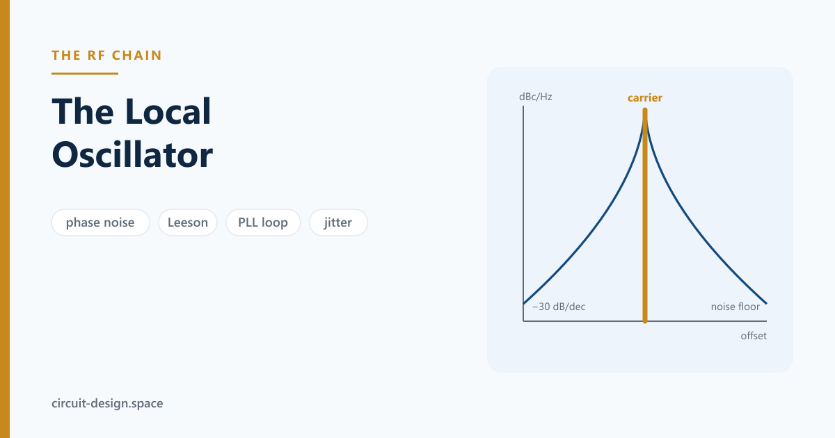
An ideal local oscillator is a pure tone. A real one is a tone with skirts — noise spread either side of the carrier — and those skirts do something specific and destructive: they convert interferers onto your signal.
1. Reciprocal mixing, which is why phase noise matters
When a mixer multiplies, it multiplies the LO’s noise skirts as well as its carrier. A strong interferer one channel away mixes with the LO noise at that offset and lands directly in your IF passband. This is reciprocal mixing, and it means LO phase noise sets your adjacent-channel blocking performance no matter how selective the IF filter is.
The integrated noise power from a skirt of density over a channel bandwidth:
| at the offset | Channel BW | Integrated noise |
|---|---|---|
| −120 dBc/Hz | 30 kHz | −75.2 dBc |
| −140 dBc/Hz | 1 MHz | −80.0 dBc |
So a −120 dBc/Hz LO with a 30 kHz channel cannot reject an adjacent interferer by more than about 75 dB, however good the rest of the receiver is. That single calculation is usually what sets the synthesizer specification.
2. Phase noise and where it comes from
is the single-sideband noise power in a 1 Hz bandwidth at offset , relative to the carrier, in dBc/Hz. The Leeson model gives the shape:
The useful content is the slopes, not the constant:
| Region | Slope | Cause |
|---|---|---|
| Close-in | −30 dB/decade | device flicker (1/f) noise up-converted |
| Mid | −20 dB/decade | thermal noise shaped by the resonator |
| Far out | flat | the noise floor of the buffer/output stage |
Three design levers fall out of it:
- Resonator appears squared. Doubling loaded Q improves the region by 6 dB. This is the whole reason a crystal beats an LC tank beats a ring oscillator.
- Signal power is in the denominator: more power in the resonator is less phase noise, which is why low-phase-noise oscillators run hot.
- The device’s flicker corner sets where the −30 dB/decade region ends. Bipolar and SiGe devices have lower than CMOS, which is why discrete low-noise oscillators are often bipolar.
3. Phase noise is jitter, in a different coordinate system
For a clock rather than an LO, the same quantity is usually quoted as RMS jitter — the integral of the phase-noise spectrum over a defined band, converted to time:
Two things follow. The integration limits are part of the number — 12 kHz to 20 MHz is the telecom convention, and a jitter figure without its band is meaningless. And because the carrier frequency is in the denominator, the same phase-noise plot gives less jitter at a higher carrier — so comparing jitter across frequencies without normalising is a mistake.
Worked, so the arithmetic is concrete. Take a flat −140 dBc/Hz floor across 12 kHz to 20 MHz on a 100 MHz clock. The integral is , doubling for both sidebands gives , and dividing by gives 1.01 ps RMS. Push the floor to −150 dBc/Hz and it becomes 0.32 ps; keep the floor and move to a 1 GHz carrier and it becomes 0.10 ps — the same oscillator quality, a tenfold better jitter number. That is the normalisation trap in one calculation.
The two things jitter then limits
A data converter’s SNR. Sampling with an uncertain clock smears a fast input, and the resulting SNR ceiling depends only on the input frequency and the jitter:
| 1 ps | 100 fs | 50 fs | |
|---|---|---|---|
| 100 MHz | 64.0 dB | 84.0 dB | 90.1 dB |
| 500 MHz | 50.1 dB | 70.1 dB | 76.1 dB |
| 1 GHz | 44.0 dB | 64.0 dB | 70.1 dB |
| 3 GHz | 34.5 dB | 54.5 dB | 60.5 dB |
Read the bottom-right corner: a 14-bit ADC sampling a 1 GHz input needs under 50 fs of total clock jitter to deliver even 11 effective bits. This is why direct-RF-sampling receivers buy their clock from a jitter cleaner and treat the clock path as a signal integrity problem — because at those numbers, it is one.
A modulation’s EVM. Residual phase error puts a floor under the constellation that no amount of transmit power removes:
| EVM floor | |
|---|---|
| 0.1° | 0.17% (−55.2 dB) |
| 0.3° | 0.52% (−45.6 dB) |
| 0.5° | 0.87% (−41.2 dB) |
| 1.0° | 1.75% (−35.2 dB) |
| 2.0° | 3.49% (−29.1 dB) |
A 1024-QAM link needs roughly −40 dB EVM from everything combined, so the synthesizer alone has to come in under about half a degree of integrated phase error. That is the requirement that the phase-noise mask exists to express, and it is worth writing down in degrees before converting it into a dBc/Hz curve — the degrees are what the modem cares about.
This is also the bridge to SerDes work: the reference clock’s phase noise becomes the transmitter’s jitter, and the receiver’s CDR has to track it.
4. The PLL
Almost every LO is a VCO locked to a reference by a phase-locked loop:
Reference (crystal or TCXO/OCXO) → phase-frequency detector → charge pump → loop filter → VCO → feedback divider → back to the PFD.
The output is , and the loop is a control system whose bandwidth is the central design trade:
Inside the loop bandwidth, the output follows the reference — so you get the reference’s phase noise, multiplied up by . That multiplication is unavoidable and is why a synthesizer’s close-in noise is always worse than its reference’s.
Outside the loop bandwidth, the loop cannot correct, and you get the VCO’s own noise.
So: a wide loop suppresses VCO noise and exposes reference noise; a narrow loop does the opposite. The optimum is where the two curves cross, and choosing it is the main act of synthesizer design. A wide loop also locks faster — lock time scales roughly as the inverse of loop bandwidth — which matters enormously for frequency-hopping and TDD systems.
The loop as a control system
For the standard type-II second-order loop with charge-pump current , VCO gain (in Hz/V) and a filter capacitor and resistor :
Three things fall out that are worth internalising:
- goes as . Change the output frequency by a large factor and the loop dynamics change with it, so a wideband synthesizer’s filter is a compromise across the band — and its worst-case damping is at one end.
- sets the peaking. An under-damped loop peaks in its closed-loop response, and that peak appears as a visible bump in the phase-noise plot near the loop bandwidth. Seeing a bump there is diagnostic: it is almost never the VCO, it is the filter. Aim for –1.0, or equivalently a phase margin of 45–60°.
- Lock time follows from the same numbers. Settling to 1 ppm takes roughly :
| Loop bandwidth | Settle to 1 ppm |
|---|---|
| 10 kHz | ≈ 620 µs |
| 100 kHz | ≈ 62 µs |
| 1 MHz | ≈ 6 µs |
A TDD system that must retune between slots, or a frequency hopper, is choosing its loop bandwidth from this table and then living with whatever phase noise that implies — the opposite of the usual direction of the argument.
Predicting in-band noise before you build it
The in-band (inside the loop bandwidth) phase noise of a synthesizer is remarkably predictable from a single normalised figure of merit that most PLL datasheets now publish:
A good modern PLL has FOM around −230 dBc/Hz, an excellent one −236. For a 4 GHz output from a 100 MHz reference (): −230 gives −118 dBc/Hz, −236 gives −124 dBc/Hz. Compare that with what the reference contributes — a −160 dBc/Hz crystal multiplied by dB lands at −128 dBc/Hz — and you have your answer about which one dominates, before choosing a part.
The structure of that formula is also the design advice: raise and lower . Both terms push the same way, which is why a 100 MHz reference beats a 10 MHz one by far more than the 10 dB you might expect.
Integer-N versus fractional-N
Integer-N: the channel spacing equals , so fine resolution forces a low reference, which forces a high (more multiplication of reference noise) and a narrow loop (worse VCO suppression, slower lock). Everything gets worse together.
Fractional-N dithers the divider between and so the average is fractional. The reference can stay high while the resolution gets fine — breaking the coupling above. The cost is fractional spurs from the periodic dithering, controlled by a delta-sigma modulator that shapes the quantisation noise to high offsets where the loop filter removes it. Modern fractional-N synthesizers are the default; their residual spurs are the thing to check on the bench, not in the datasheet.
The modulator order is a real choice and it is not “higher is better”. An order- modulator shapes its quantisation noise upward at dB/decade:
| Modulator order | Slope above the loop corner | Behaviour |
|---|---|---|
| 1 | flat | strong, tonal spurs — effectively unusable |
| 2 | 20 dB/decade | quiet, but can produce tones at simple fractions |
| 3 | 40 dB/decade | the common default; well randomised |
| 4 | 60 dB/decade | best close-in, and it demands a narrow loop to stay quiet far out |
So the modulator order and the loop bandwidth are one decision, not two: a high-order modulator dumps a great deal of noise just above the loop corner, and the filter has to remove it. Choosing a 4th-order modulator and then widening the loop for fast lock is a classic way to build a synthesizer that is noisier than the 3rd-order version it replaced.
Integer-boundary spurs are the fractional-N failure mode worth knowing by name. When the fractional part of is very close to an integer, the dithering becomes nearly periodic at a very low rate, and the resulting spur sits inside the loop bandwidth where the filter cannot touch it. Every wideband fractional-N synthesizer has output frequencies where this happens, and the datasheet usually shows them as spikes on a spur-versus-frequency plot. The fix is a frequency plan that avoids those output frequencies, or a reference that can be shifted to move them — and both need to be known before the plan is fixed.
5. VCO topologies
| Topology | Phase noise | Tuning range | Where |
|---|---|---|---|
| LC cross-coupled | good | 10–30% | the integrated default |
| Colpitts | very good | moderate | discrete and SiGe low-noise designs |
| Ring oscillator | poor | very wide | digital clocking, not RF |
| Crystal / OCXO | excellent | almost none | references, not tunable LOs |
| YIG | excellent | multi-octave | instrumentation, slow tuning |
| DDS | set by the DAC/clock | instant, fine | agile sources, spur-limited |
The recurring trade is tuning range against phase noise, because wide tuning means a large varactor, and a large varactor means the tank Q falls and the VCO gain rises — and a high converts every millivolt of noise on the tune line into phase noise. Switched capacitor banks exist precisely to get range without a huge varactor: coarse steps digitally, fine tuning with a small varactor.
Two datasheet parameters that decide your layout
Pushing (, MHz/V) is how much the output frequency moves with the supply. Pulling is how much it moves with the load impedance, usually specified into a 12 dB return loss at all phases. They are not footnotes — they are the two mechanisms by which a perfectly good VCO becomes a spur generator on a real board.
For a small sinusoidal disturbance the result is narrowband FM, and the sideband level is:
which converts supply ripple straight into dBc. At 500 kHz — a perfectly ordinary switching regulator frequency:
| 0.1 mVpk | 1 mVpk | 10 mVpk | |
|---|---|---|---|
| 1 MHz/V | −80 dBc | −60 dBc | −40 dBc |
| 5 MHz/V | −66 dBc | −46 dBc | −26 dBc |
| 20 MHz/V | −54 dBc | −34 dBc | −14 dBc |
One millivolt of ripple on a 5 MHz/V VCO is a −46 dBc spur. One millivolt is not a design error — it is what you get from a decent LDO with a switcher in front of it, and it is far below anything that would look wrong on a scope. That table is the entire justification for giving a VCO its own regulator, its own ferrite, and a tune line routed away from everything that switches; see power integrity for how to get the ripple itself down.
The same arithmetic applied to pulling explains why a VCO that meets its specification on the bench can fail in the system: a buffer amplifier between the VCO and a varying load costs a little power and removes the mechanism entirely.
6. Spurs
Distinct from phase noise — discrete tones rather than a continuum, and each has a findable cause:
| Spur | Offset | Cause |
|---|---|---|
| Reference spur | at | charge-pump mismatch and leakage |
| Fractional spur | at fractional offsets | divider dithering |
| Supply / ground | at the switcher frequency | poor PSRR on the VCO or tune line |
| Mechanical | low offset | microphonics — a real problem in cavity and crystal oscillators |
Supply-borne spurs deserve special mention because they are the most common and the most avoidable: a switching regulator ripple on a VCO supply or tune line modulates the frequency directly — at the rate the table in §5 quantifies. Give the VCO its own clean rail, and see power integrity.
Reference spurs have a specific and findable cause: charge-pump up/down current mismatch, and leakage on the tune node. Both produce a correction pulse once per reference cycle even when the loop is locked, which frequency-modulates the VCO at . Two practical consequences. Mismatch is worst at the extremes of the charge-pump’s output voltage range, so a VCO whose tune voltage sits near a rail will show worse reference spurs than the same part tuned to mid-range — a spur that varies with output frequency and vanishes in the middle of the band is nearly always this. And leakage matters because the tune node is high-impedance: nanoamps through a dirty board, a poorly chosen capacitor dielectric, or a varactor’s own reverse leakage are enough. Clean and conformal-coat the loop filter area, and use C0G/NP0 rather than X7R for the filter capacitors — the dielectric absorption in X7R is itself a spur mechanism.
7. A design method
- Derive the phase-noise mask from the system: reciprocal-mixing blocking, EVM for the modulation, or jitter for a data converter.
- Choose the reference. Its noise, multiplied by , is your close-in floor.
- Choose fractional-N or integer-N from the resolution and lock-time requirement.
- Pick the VCO on tuning range and its own phase noise at the offsets that matter.
- Set the loop bandwidth where the reference-multiplied curve crosses the VCO curve.
- Design the loop filter for that bandwidth with adequate phase margin — an under-damped loop peaks, and the peak shows up as a bump in the phase-noise plot.
- Isolate the supplies, especially the tune line.
- Measure phase noise, spurs and lock time, and look for the peak that says the loop is under-damped.
8. Example parts
The synthesizer market is unusually well served, and the right move is nearly always to buy an integrated PLL+VCO rather than build a discrete loop — unless the phase-noise requirement is extreme, in which case nothing integrated will do. Check current availability; these are illustrative.
Integrated PLL + VCO — one part, a reference, a loop filter and an SPI bus:
| Part | Output range | Why you would pick it |
|---|---|---|
| Analog Devices ADF4351 | 35 MHz–4.4 GHz | the ubiquitous hobby-to-production wideband synth; enormous ecosystem |
| Analog Devices ADF4355 | 54 MHz–6.8 GHz | the modern successor, noticeably better phase noise |
| Analog Devices ADF5355 | 54 MHz–13.6 GHz | when the plan needs microwave from one part |
| Texas Instruments LMX2594 | 10 MHz–15 GHz | very low in-band noise and fast lock; the current benchmark for wideband |
| Texas Instruments LMX2572 | 12.5 MHz–6.4 GHz | lower power, with a built-in ramp generator for FMCW radar |
Clock generation and jitter cleaning — the parts to reach for when the destination is an ADC rather than a mixer:
| Part | Why you would pick it |
|---|---|
| Texas Instruments LMK04828 | dual-loop jitter cleaner with JESD204B support; sub-100 fs territory |
| Analog Devices HMC7044 | 14-output clock distribution with a cleaning PLL — the RF-sampling default |
| Skyworks Si5341 | any-frequency multi-output clock generator, very flexible |
References and discrete VCOs — where the close-in noise is actually decided:
| Part family | Why you would pick it |
|---|---|
| Abracon ASTX / ASVTX TCXO | ±0.5–2.5 ppm over temperature in a small package; the usual portable reference |
| Connor-Winfield / Rakon OCXO | ±5–50 ppb and far better close-in noise, at real power and warm-up cost |
| Crystek CVCO55 series | discrete coaxial-resonator VCOs, better phase noise than any integrated tank |
The selection rule, stated plainly: the reference decides your close-in noise and the VCO decides your far-out noise, and the PLL’s own FOM decides the floor between them. Buying an excellent synthesizer and clocking it from a cheap crystal is the most common way to waste money on this page — that multiplies whatever you feed it.
9. The pitfalls
- Quoting jitter without its integration band.
- Comparing jitter across different carrier frequencies without normalising.
- A loop bandwidth chosen by default rather than from the crossover.
- Switching-regulator ripple on the VCO supply or tune line.
- Forgetting that multiplies reference noise by — 40 dB at .
- Fractional spurs assumed absent because the datasheet plot did not show them.
- Microphonics in a design that will be in a vibrating environment.
- Choosing a high-order delta-sigma modulator and a wide loop, and getting a noisier synthesizer than the simpler version.
- A frequency plan that sits on an integer boundary, where the spur is inside the loop bandwidth and unfilterable.
- X7R capacitors in the loop filter, and a tune node that leaks.
- An excellent PLL fed by a cheap reference.
Further reading
- Randall Rhea, Discrete Oscillator Design. The practical book on building oscillators that work, rather than analysing ones that do.
- Dean Banerjee, PLL Performance, Simulation and Design. The loop-filter and spur reference; the normalised-FOM arithmetic above comes from this tradition.
- Ulrich Rohde, Microwave and Wireless Synthesizers: Theory and Design. Exhaustive, and the place to go when the standard treatment runs out.
- Behzad Razavi, RF Microelectronics. Integrated VCOs and fractional-N synthesis from the silicon side.
- D. B. Leeson, “A simple model of feedback oscillator noise spectrum”, Proc. IEEE 54(2), 1966 — four pages, and still the model everyone uses.
The RF chain, block by block —Antenna · Filter · LNA · Mixer · LO · IF & ADC · PA · Isolator · Coupler · Overview
Glossary
Damping and loop peaking — A loop with too little phase margin peaks in its closed-loop response, and the peak appears as a visible bump in the phase-noise plot near the loop bandwidth. Seeing a bump there is diagnostic: it is almost never the VCO, it is the filter. Aim for –1.0, or 45–60° of phase margin.
Delta-sigma modulator — What dithers a fractional-N divider so its quantisation noise is shaped to high offsets where the loop filter removes it. Order- shaping rises at dB/decade, so the modulator order and the loop bandwidth are one decision: a 4th-order modulator with a wide loop is noisier than the 3rd-order version it replaced.
Integer-boundary spur — When the fractional part of sits very close to an integer the dithering becomes nearly periodic, and the resulting spur lands inside the loop bandwidth where the filter cannot touch it. Every wideband fractional-N part has output frequencies where this happens; the fix is a frequency plan that avoids them.
Jitter integration band — The limits over which phase noise is integrated to give an RMS jitter figure; 12 kHz to 20 MHz is the telecom convention. A jitter number without its band is meaningless, and because the carrier is in the denominator the same oscillator gives a better number at a higher frequency.
— Tuning sensitivity in Hz/V. Wide tuning needs a big varactor, which lowers tank Q and raises — and a high converts every millivolt of noise on the tune line into phase noise. Switched capacitor banks exist to get range without paying it.
Leeson model — The standard oscillator phase-noise shape: −30 dB/decade close in from up-converted flicker, −20 dB/decade from thermal noise shaped by the resonator, then flat. The useful content is the slopes and the three levers — loaded (squared), resonator power, and the device’s flicker corner.
Lock time — Roughly , and inversely proportional to loop bandwidth: about 620 µs at a 10 kHz loop, 6 µs at 1 MHz. A frequency hopper or a TDD system chooses its loop bandwidth from this and lives with whatever phase noise follows — the opposite of the usual direction of the argument.
PLL figure of merit — The normalised constant in , around −230 dBc/Hz for a good part. It lets you predict in-band noise before choosing anything, and its structure is the design advice: raise , lower .
Pulling — Frequency shift caused by a varying load, usually specified into a 12 dB return loss at all phases. A buffer between the VCO and anything that moves costs a little power and removes the mechanism, which is why a VCO that meets spec on the bench can fail in the system.
Pushing () — Frequency shift with supply voltage, in MHz/V. One millivolt of ripple on a 5 MHz/V VCO at 500 kHz is a −46 dBc spur — and one millivolt is what a decent LDO with a switcher in front of it delivers. The entire justification for giving a VCO its own regulator.
Reciprocal mixing — The mechanism that makes phase noise matter: a mixer multiplies the LO’s noise skirts as well as its carrier, so a strong adjacent interferer mixes with the skirt at that offset and lands in the IF. It sets blocking performance regardless of how selective the IF filter is.
Reference spur — A discrete tone at from charge-pump mismatch and tune-node leakage. Worst when the tune voltage sits near a rail, so a spur that varies with output frequency and vanishes mid-band is nearly always this. C0G rather than X7R in the loop filter, and keep the node clean.
VCO topology — LC cross-coupled for integration, Colpitts for low noise, ring for digital clocking, crystal/OCXO for references, YIG for instrumentation. The recurring trade is tuning range against phase noise, because range means a large varactor and a large varactor means low tank Q.
Related
- The RF chain overview
- The mixer it drives — LO drive level and reciprocal mixing
- Power integrity — where supply-borne spurs come from
- Signal integrity — where phase noise becomes transmitter jitter
Have a synthesizer that will not meet its mask, or spurs nobody can source? That’s what we do. Reach us at circuit-design.space.
circuit-design.space · +1-971-357-1400 · anovickis@circuit-design.space