Part of the RF chain series — a page per block. The PA feeds the isolator, then the coupler, then the antenna.
The RF chain, block by block —Antenna · Filter · LNA · Mixer · LO · IF & ADC · PA · Isolator · Coupler · Overview
Everything else in the chain handles signals small enough that the devices behave linearly. The PA does not, and cannot — a power amplifier operated in its linear region is a power amplifier wasting most of its supply as heat. Every PA design is a negotiation between efficiency and linearity, and there is no position on that axis that is free.
1. The measures
| Parameter | Meaning |
|---|---|
| P1dB | Output power where gain has compressed 1 dB — the practical top of linear operation |
| Psat | Saturated output power |
| PAE | Power-added efficiency, |
| Drain/collector efficiency | — flattering, because it ignores drive |
| OIP3 | Output third-order intercept |
| ACPR | Adjacent-channel power ratio — spectral regrowth into the neighbours |
| EVM | Error vector magnitude — what the constellation sees |
| Ruggedness | Survival into a load VSWR, typically 10:1 at all phases |
PAE is the honest one. Drain efficiency ignores the drive power, which for a low-gain device at millimetre-wave is a large fraction of the total. A 3 dB gain stage with 60% drain efficiency has far worse PAE than that number suggests.
2. The classes
Conduction angle — how much of the RF cycle the device conducts for — sets the first family:
| Class | Conduction | Max efficiency | Linearity | Where |
|---|---|---|---|---|
| A | 360° | 50% | best | small-signal drivers, instrumentation |
| AB | 180–360° | 50–78% | good | the workhorse for modulated signals |
| B | 180° | 78.5% | moderate | push-pull audio and RF |
| C | < 180° | > 78% | poor | constant-envelope only — FM, CW |
Class C is only usable when the signal has no amplitude information. Any modern modulation with amplitude variation — QAM, OFDM — cannot use it.
Where those efficiency numbers come from
The whole family drops out of one piece of arithmetic, and it is worth doing once because it also tells you what you lose along with what you gain. Take the device’s drain current as a truncated cosine conducting for a full angle , and take the Fourier components:
With a full voltage swing the efficiency is simply :
| Class | Fundamental vs class A | ||||
|---|---|---|---|---|---|
| A | 360° | 0.500 | 0.500 | 50.0% | 0 dB |
| AB | 260° | 0.431 | 0.535 | 62.1% | +0.59 dB |
| AB | 200° | 0.349 | 0.520 | 74.4% | +0.34 dB |
| B | 180° | 0.318 | 0.500 | 78.5% | 0 dB |
| C | 120° | 0.218 | 0.391 | 89.7% | −2.14 dB |
| C | 90° | 0.165 | 0.310 | 94.0% | −4.15 dB |
The column on the right is the one people do not expect. Deep class AB delivers more fundamental power than class A from the same device — up to about 0.6 dB more — because truncating the current waveform concentrates energy in the fundamental even as it reduces the mean. You get more power and better efficiency, and you pay in linearity. That is why class AB is not a compromise between A and B so much as the actual operating point of nearly every practical linear PA.
Note also how flat efficiency is across the AB region and how steeply output power falls once you push into C. Between 200° and 180° the efficiency gains 4 points and the output barely moves; between 120° and 90° the output drops 2 dB for 4 points. The useful territory is 180–260°, and everything outside it is either wasteful or a different kind of amplifier.
The switching classes stop treating the device as a controlled current source and start treating it as a switch, shaping the harmonic terminations so the device never has high voltage and high current simultaneously:
| Class | Idea | Efficiency | Catch |
|---|---|---|---|
| D | switching pair | > 90% theoretical | switching losses, device capacitance |
| E | single switch with a tuned load that shapes zero-voltage switching | > 90% | narrowband, sensitive to load |
| F | harmonic termination — short even, open odd harmonics (or inverse) | > 85% | needs a real harmonic-controlled output network |
Class F is worth understanding as the general principle: you get efficiency by controlling where the harmonics go, not just the fundamental. The output network is a multi-frequency design problem, and simulating it needs harmonic balance, not a fundamental-only match.
3. Load-pull: the optimum load is not the conjugate match
This is the single most important idea in PA design and the one most often got wrong.
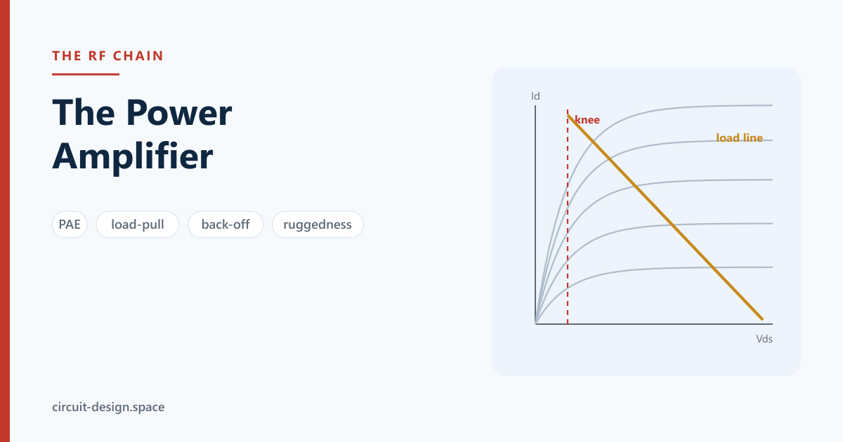
For a small-signal amplifier, maximum power transfer comes from conjugate matching the output. For a PA it does not — because the device is voltage- and current-limited, not source-impedance-limited. The load that extracts maximum power is the one that lets the device swing to its voltage limit exactly as it reaches its current limit. Approximately:
which is usually far lower than the device’s own output impedance. Worked, across the range of designs you actually meet:
| 28 V | 3 V | 10 W | 31.3 Ω |
| 28 V | 3 V | 25 W | 12.5 Ω |
| 50 V | 5 V | 100 W | 10.1 Ω |
| 5.0 V | 0.5 V | 2 W | 5.1 Ω |
| 3.4 V | 0.3 V | 1 W | 4.8 Ω |
Two things to take from that table.
The high-voltage technologies exist because of the square in the numerator. A 100 W amplifier at 50 V wants 10 Ω; at 28 V it would want 3.1 Ω, and at a handset’s 3.4 V it would want 0.05 Ω — an impedance you cannot match with any real network without losing most of the power in the match itself. That is the whole argument for GaN at 50 V in base stations, and the reason a handset PA’s output match is a genuinely difficult 5:1 transformation done in millimetres.
The knee voltage is not a detail. At a 3.4 V supply, a 0.3 V knee removes 8.8% of the available swing and 0.80 dB of output power — and a device with a 0.6 V knee would cost 1.7 dB. Low-voltage PA design is largely a fight with the knee, which is why device technologies get compared on knee voltage as seriously as on breakdown.
Load-pull measures or simulates output power and efficiency as the presented load is swept across the Smith chart, producing contours of constant power and constant PAE. Two things come out of it:
- The maximum-power load and the maximum-efficiency load are different points. Choosing between them, or somewhere on the line between, is a system decision.
- The contours’ shape tells you the sensitivity — how much performance you lose for a given load error, which sets how tight the output match and the antenna VSWR need to be.
Source-pull does the same for the input, and matters for gain and stability.
4. Back-off, and the efficiency problem it creates
Modern modulation has a high peak-to-average power ratio, and the number varies more than people expect:
| Signal | PAPR |
|---|---|
| GMSK, FM — constant envelope | 0 dB |
| QPSK with root-raised-cosine shaping | 3–4 dB |
| 16-QAM, single carrier | 5–6 dB |
| LTE uplink (SC-FDMA) | 6–7 dB |
| LTE / 5G OFDM downlink | 8–12 dB |
| 802.11ax OFDMA | 10–12 dB |
To avoid clipping the peaks, the PA runs its average power that far below saturation. And efficiency falls with back-off in a way that is easy to underestimate, because in a current-source-mode amplifier the voltage swing falls with the signal while the DC current does not fall as fast:
| Back-off | Ideal class B | Ideal class A |
|---|---|---|
| 0 dB | 78.5% | 50.0% |
| 3 dB | 55.6% | 25.1% |
| 6 dB | 39.4% | 12.6% |
| 8 dB | 31.3% | 7.9% |
| 10 dB | 24.8% | 5.0% |
| 12 dB | 19.7% | 3.2% |
Those are ideal numbers with no knee, no loss and no quiescent current; a real class-AB PA at 8 dB back-off typically lands nearer 15% against the 31% here. Note the exponents: class B loses efficiency as and class A as — class A degrades twice as fast in dB terms, which is why nobody runs a high-PAPR signal through a class-A stage.
This table is the entire commercial case for Doherty and envelope tracking. A base station transmitting a 10 dB-PAPR signal from a plain class-AB PA turns three quarters of its supply into heat, and at the scale of a national network that is a line item large enough to fund a lot of engineering.
Three responses, all in production use:
Digital pre-distortion (DPD). Characterise the PA’s nonlinearity and apply the inverse in the digital domain, so the PA can run closer to compression while the system stays linear. Needs a feedback path — which is what the directional coupler is for — and enough DSP. Now standard in cellular infrastructure.
Doherty. Two amplifiers: a main (class AB) always on, and a peaking (class C) that turns on only for peaks, with a quarter-wave line performing active load modulation. Restores efficiency at back-off. The dominant base-station architecture.
The mechanism is worth stating precisely, because “two amplifiers” undersells it. Below the turn-on point the peaking device is off and presents an open, and the quarter-wave inverter transforms that into a higher load for the main device — so the main device reaches its voltage limit at a lower output power, which is exactly the condition for peak efficiency. As the peaking device turns on it injects current into the common node, lowering the impedance the main device sees, and the main device stays saturated while the pair delivers more power. Efficiency peaks twice: once at the designed back-off point and once at full power, with a shallow dip between. A classical symmetric Doherty peaks at 6 dB back-off; asymmetric and three-way designs push that to 9 or 12 dB to match modern PAPR, at the cost of bandwidth and of a more delicate peaking-device turn-on.
Its weaknesses are also specific: the quarter-wave inverter is narrowband (typically 5–15% for full performance), the class-C peaking stage is nonlinear by construction so Doherty essentially requires DPD, and the turn-on characteristic drifts with temperature and process.
Envelope tracking. Modulate the supply voltage to follow the signal envelope, so the device is never over-supplied — in effect keeping matched to the instantaneous swing instead of to the peak. Common in handsets, where the modulator’s own efficiency and bandwidth are the difficulty: it has to track several times the signal bandwidth, and a switching modulator fast enough to do that puts ripple exactly where the receiver is listening.
Outphasing (LINC / Chireix) is the fourth option and appears occasionally: split the signal into two constant-envelope phase-modulated components, amplify both with efficient saturated stages, and recombine. Beautiful on paper; the combiner and the path-matching requirement are what keep it rare.
5. Ruggedness and the thing that kills PAs
A PA sees whatever the antenna reflects. An antenna that is detuned, iced, blocked by a hand, or disconnected presents a high VSWR, and at some phase angle that load maximises either voltage or current at the device — beyond its rating.
This is what the isolator exists for. With 20 dB of isolation:
| Load VSWR | at the load | PA sees | PA sees VSWR |
|---|---|---|---|
| 2.0 | 0.333 | 0.033 | 1.069 |
| 3.0 | 0.500 | 0.050 | 1.105 |
| 10.0 | 0.818 | 0.082 | 1.178 |
A catastrophic 10:1 load becomes a benign 1.18:1 at the device. That is why transmit chains that must survive an open or shorted antenna put a ferrite isolator after the PA, and accept its 0.3–0.5 dB of forward loss as insurance.
Where an isolator is not affordable, the alternative is a VSWR protection loop: the coupler measures reflected power and the control system backs off drive.
6. Thermal design is reliability design
At 30% PAE, more than twice the RF output is leaving as heat. For a 10 W amplifier:
| PAE | DC in | Dissipated |
|---|---|---|
| 25% | 40.0 W | 30.0 W |
| 30% | 33.3 W | 23.3 W |
| 45% | 22.2 W | 12.2 W |
| 60% | 16.7 W | 6.7 W |
That heat sets junction temperature through a stack of thermal resistances in series:
and the arithmetic is unforgiving. The same 23.3 W of dissipation, three plausible stack-ups:
| Ambient | ||||
|---|---|---|---|---|
| 1.5 | 0.3 | 1.0 | 25 °C | 90 °C |
| 1.5 | 0.3 | 2.5 | 55 °C | 155 °C |
| 3.0 | 0.5 | 2.5 | 55 °C | 195 °C |
Same amplifier, same power, and the difference between comfortable and over the rating is a slightly worse device package, a thermal-interface material that was chosen by the mechanical team, and an ambient that reflects where the box actually lives. Note that the case-to-sink term is the one most often guessed at and the one you fully control: a badly applied thermal pad can be worth more than the difference between two device families.
Junction temperature then sets both performance — gain and output power fall as it rises, which is why a PA’s measured power droops over the first seconds of a transmit burst — and lifetime. Wear-out follows Arrhenius:
With a typical eV near 175 °C, every 10 °C of junction temperature costs roughly a factor of 1.8 in lifetime — very close to the familiar “10 degrees halves the life” rule. A 20 °C error in a thermal estimate is a 3× error in the reliability prediction, which is the argument for simulating the thermal path rather than applying a rule of thumb. The same exponential appears in Black’s equation for electromigration on the supply metal that feeds the device.
The practical points: thermal vias directly under the device pad, a real copper path to the enclosure or heatsink, thermal simulation rather than a guess, and — critically — thermal and RF design interact, because the via field and pad geometry that carry heat are part of the RF output network. A via array added late for thermal reasons will detune a match that was closed months earlier.
Device technology also matters here: GaN tolerates far higher junction temperatures and power densities than LDMOS or GaAs, which is why it took over high-power applications despite costing more. And the substrate matters as much as the semiconductor — GaN-on-SiC conducts heat several times better than GaN-on-Si, which is why the expensive one exists.
7. Bias sequencing, which destroys more GaN than anything else
This belongs in the practical section rather than the theory, because it is a production problem rather than a design one, and it kills parts.
GaN HEMTs and GaAs pHEMTs are depletion-mode devices: they conduct at zero gate voltage. Apply the drain supply before a negative gate bias and the device conducts hard, with no current limiting but its own knee, and it is gone in microseconds. So:
- Power up: negative gate first, verify it, then drain. Ramp the gate toward the operating point last, watching the quiescent current.
- Power down: exactly the reverse — drain off first, gate last.
- Protect against a lost gate supply. If the negative rail fails or is slow to come up while the drain rail is present, you have the failure case above. A supervisor that holds the drain switch off until the gate rail is in range costs very little and prevents the whole class.
- Set quiescent current, not gate voltage. for a given varies substantially part to part and drifts with temperature. Production designs use an active bias loop that regulates ; open-loop gate voltage means the class of operation — and therefore the linearity — is different on every unit and at every temperature.
Enhancement-mode devices (LDMOS, E-pHEMT, and enhancement-mode GaN) avoid the sequencing hazard, which is a real part of why they are chosen for high-volume products.
8. A design method
- Establish the output power including the PAPR back-off the modulation requires, and the ACPR/EVM mask.
- Choose the technology — LDMOS, GaAs, GaN, SiGe — on frequency, power and thermal budget.
- Choose the class and architecture from the linearity requirement and whether DPD is available.
- Load-pull to find the optimum load for power and for efficiency; decide where to sit.
- Design the output network to present that impedance at the fundamental and the intended terminations at the harmonics.
- Check stability, in and out of band, with the real bias network. A PA has enormous low-frequency gain.
- Simulate with harmonic balance and envelope for ACPR and EVM.
- Design the thermal path and simulate it.
- Test into VSWR at all phase angles, not just into 50 Ω.
9. Example parts, by technology
The technology choice comes first and it narrows the field to a handful. Illustrative parts — check availability and the current datasheet.
GaN — high voltage, high power density, high junction temperature. The default for new high-power designs:
| Part | Notes |
|---|---|
| Wolfspeed CGH40010F | 10 W, DC–6 GHz, 28 V — the classic evaluation device, and an enormous body of published designs |
| Wolfspeed CGHV1F025S | 25 W at 50 V, for when needs the higher rail |
| Analog Devices HMC1099 | 10 W GaN MMIC, 0.01–1.1 GHz — matched, so no output network to design |
| Qorvo TGA2598 | GaN MMIC for X-band and up |
LDMOS — the incumbent at VHF/UHF and cellular infrastructure, cheap per watt, enormous power available, and limited in frequency:
| Part | Notes |
|---|---|
| NXP MRFE6VP5600H | 600 W, to 600 MHz, and rated to survive a 65:1 load mismatch |
| NXP MRFX1K80H | 1.8 kW HF/VHF — the broadcast and industrial-heating class |
GaAs / SiGe MMIC and gain blocks — matched, easy, and the right answer below a few watts:
| Part | Notes |
|---|---|
| Mini-Circuits PHA-1+ | 0.05–6 GHz, +23 dBm, high IP3 — a very good general-purpose driver |
| Mini-Circuits GVA-84+ | broadband gain block for driving a bigger stage |
| Qorvo TQP7M9103 | 0.05–4 GHz driver with good linearity per milliamp |
| Skyworks SKY66 series | integrated front-end modules — PA, switch and often an LNA in one part |
For anything under a couple of watts in a standard band, look hard at the front-end modules before designing a discrete PA. They arrive matched, characterised, with the harmonic filter and the switch included, and they will beat a discrete design on size, cost and schedule. Discrete design earns its place when the power, the band, the ruggedness or the efficiency requirement is outside what anyone has integrated.
Two things to check on any datasheet before committing: the load-pull data (if the manufacturer publishes contours, the design is half done; if they do not, budget for measuring them) and the ruggedness specification (which load VSWR, at what drive, for how long — the three numbers are frequently not all printed).
10. The pitfalls
- Conjugate-matching the output and wondering where the power went.
- Quoting drain efficiency and calling it PAE.
- Class C with an amplitude-modulated signal.
- Fundamental-only output matching on a switching-class design.
- Ignoring the harmonic terminations and losing the efficiency the class was chosen for.
- Testing only into 50 Ω, then failing in the field on a detuned antenna.
- A thermal path designed after the RF network, forcing a compromise on both.
- Low-frequency instability in the bias network — the most common PA oscillation.
- Applying drain before gate on a depletion-mode device, once.
- Setting gate voltage instead of regulating quiescent current, and shipping units with different classes of operation.
- A thermal stack-up estimated rather than simulated, then a reliability prediction built on it.
- Adding a thermal via array after the output match was closed.
Further reading
- Steve Cripps, RF Power Amplifiers for Wireless Communications. The book. The reduced-conduction-angle analysis and the load-line argument above are his presentation, and nobody has improved on it.
- Steve Cripps, Advanced Techniques in RF Power Amplifier Design. Switching classes, Doherty and harmonic termination in depth.
- Andrei Grebennikov, RF and Microwave Power Amplifier Design. Broad, formula-dense, and good on the switching classes.
- Guillermo Gonzalez, Microwave Transistor Amplifiers: Analysis and Design. For the stability analysis that a PA needs as much as an LNA does.
- Fadhel Ghannouchi and Mohammad Hammi, Behavioral Modeling and Predistortion of Wideband Wireless Transmitters. If DPD is part of your system rather than someone else’s.
The RF chain, block by block —Antenna · Filter · LNA · Mixer · LO · IF & ADC · PA · Isolator · Coupler · Overview
Glossary
Bias sequencing — On a depletion-mode device (GaN HEMT, GaAs pHEMT) the gate must be negative before the drain supply arrives and must survive until after it leaves. Get it backwards once and the device is gone in microseconds. The reason production designs hold the drain switch off until the negative rail is in range.
Conduction angle — The fraction of the RF cycle the device conducts for, and the parameter that defines classes A through C. The useful territory is 180–260°: deep class AB delivers about 0.6 dB more fundamental power than class A as well as better efficiency, and you pay in linearity.
Doherty — A main amplifier always on and a peaking amplifier that turns on only for peaks, with a quarter-wave inverter performing active load modulation. Efficiency peaks twice — at the designed back-off point and at full power — which is why it dominates base stations. Narrowband, and it essentially requires DPD.
Drain efficiency — . Flattering, because it ignores the drive power the stage consumed; PAE charges for it. On a low-gain millimetre-wave device the difference is large, and a datasheet quoting drain efficiency as “efficiency” is being optimistic.
Envelope tracking — Modulating the supply to follow the signal envelope, so the device is never over-supplied. Common in handsets; the difficulty is the modulator, which must track several times the signal bandwidth and whose own switching lands where the receiver listens.
Harmonic termination — Controlling where the harmonics go, not just the fundamental. The general principle behind the switching classes: class F shorts the even harmonics and opens the odd ones so the device never has high voltage and high current at once.
Knee voltage () — The drain voltage below which the device stops behaving as a current source. It subtracts directly from the available swing, so at a handset’s 3.4 V a 0.3 V knee costs 0.80 dB of output power — which is why device technologies are compared on knee voltage as seriously as on breakdown.
Load line — The locus of (voltage, current) the device traverses for a given load. The optimum load is the one whose line reaches the voltage limit and the current limit together; the conjugate match is a higher resistance whose line is voltage-limited with current capability unused.
PAPR — Peak-to-average power ratio: 0 dB for constant envelope, 3–4 dB for shaped QPSK, 8–12 dB for OFDM. It sets the back-off, which sets the efficiency, which is why modulation choice is a thermal decision as much as a spectral one.
Psat vs P1dB — Saturated output power and the 1 dB compression point. P1dB is the practical top of linear operation; Psat is what the device can produce when linearity has stopped mattering. Quoting Psat for a linear application overstates usable power by several dB.
— Approximately : the load that extracts maximum power, and usually far below the device’s own output impedance. The square in the numerator is the entire argument for 50 V GaN in base stations and the reason a handset PA’s output match is a difficult transformation done in millimetres.
Ruggedness — Survival into a load mismatch, typically 10:1 at all phases. Three numbers make a real specification — which VSWR, at what drive, for how long — and datasheets frequently print only one of them.
Thermal resistance () — Junction-to-case, case-to-sink and sink-to-ambient in series. The case-to-sink term is the one most often guessed at and the one you fully control: a badly applied thermal pad can be worth more than the difference between two device families.
Related
- The RF chain overview
- The isolator after it — what makes a 10:1 load survivable
- The coupler — the feedback path DPD and VSWR protection need
- The antenna — the load that is never quite 50 Ω
- The Smith chart — where load-pull contours live
Have a PA that will not meet its ACPR, or a transmit chain that does not survive a detuned antenna? That’s what we do. Reach us at circuit-design.space.
circuit-design.space · +1-971-357-1400 · anovickis@circuit-design.space