Second in a five-part series. Part one covered signal integrity — the channel, the connector, and which solver to reach for. Part three covers RF and microwave design. Parts four and five move inside the die: on-die signal integrity and silicon power usage.
Power integrity answers a question that sounds trivial and is not: is the voltage at every transistor, at every instant, inside the window that transistor needs?
It is not trivial because the two halves of that question have almost nothing to do with each other. The static half is Ohm’s law over a complicated shape, and it is dominated by copper geometry, current density and temperature. The dynamic half is a resonant network spanning eight decades of frequency, and it is dominated by inductance — an inductance you mostly cannot see on the schematic, because it lives in mounting geometry, plane spreading, package balls and on-die metal.
Teams that are good at one and not the other are common. Boards fail both ways.
Part I — Static: IR drop, current density, and heat
1. The arithmetic
Static power integrity is Ohm’s law applied to a distributed conductor:
Copper foil weight, converted once so you stop converting it:
| Foil weight | Thickness | Sheet resistance |
|---|---|---|
| ½ oz | 17.4 µm | 0.966 mΩ/sq |
| 1 oz | 34.8 µm | 0.483 mΩ/sq |
| 2 oz | 69.6 µm | 0.241 mΩ/sq |
“Ohms per square” is the useful abstraction: resistance depends on the number of squares along the current path, not on absolute size. A 2 mm-wide, 50 mm-long 1 oz trace is 25 squares — 12.1 mΩ. At 3 A that is 36 mV of drop and 109 mW of heat in the copper.
| Geometry | Foil | R | Current | Drop | Dissipation |
|---|---|---|---|---|---|
| 2 mm × 50 mm | 1 oz | 12.07 mΩ | 3 A | 36.2 mV | 109 mW |
| 5 mm × 100 mm | 2 oz | 4.83 mΩ | 10 A | 48.3 mV | 483 mW |
| 0.5 mm × 20 mm | 1 oz | 19.31 mΩ | 1 A | 19.3 mV | 19 mW |
Now put that against a modern core rail. A 0.8 V rail with a ±3% tolerance has 24 mV of total budget for everything: VRM setpoint error, remote-sense error, board drop, package drop, and on-die drop. The 36 mV in the first row of that table has already spent the entire budget, twice over, before the current reaches the package. This is why high-current rails are plane-fed and not trace-fed, why remote sense exists, and why “just make the trace wider” stops being an available answer.
2. Vias are part of the resistance
A single via barrel is small but not negligible, and current rails cross layers repeatedly:
| Barrel Ø | Plating | Board thickness | Barrel R |
|---|---|---|---|
| 0.20 mm | 25 µm | 1.6 mm | 1.52 mΩ |
| 0.30 mm | 25 µm | 1.6 mm | 1.05 mΩ |
| 0.10 mm | 20 µm | 0.8 mm | 1.78 mΩ |
One 0.3 mm via at 1 mΩ carrying 10 A drops 10 mV and dissipates 100 mW into a structure the size of a grain of sand. Via count on a power rail is a design parameter, not a routing convenience — and the vias must be distributed across the current front, not clustered at one corner where the plane’s spreading resistance then does the damage.
3. Temperature makes it worse, and heat is coupled
Copper resistivity rises about 0.393% per °C:
| Temperature | ρ vs. 20 °C |
|---|---|
| 25 °C | +2.0% |
| 85 °C | +25.5% |
| 125 °C | +41.3% |
A rail that just passes at 25 °C is 25% worse at 85 °C. Worse, the mechanism is self-reinforcing: more resistance produces more heat produces more resistance. Any serious DC analysis is therefore an electrothermal analysis — solve the current distribution, compute the dissipation, solve the thermal field, update the resistivity, iterate. Tools that offer coupled DC-thermal iteration are offering it because the uncoupled answer is optimistic.
Trace current-carrying capacity comes from IPC-2152 (the modern, measurement-based standard, which accounts for copper weight, plane proximity and board thermal conductivity) rather than the older IPC-2221 charts, which are conservative in some regimes and non-conservative in others.
4. Electromigration
At high current density, metal atoms migrate along the electron flow, thinning the conductor until it opens. It is a wear-out mechanism with a mean time to failure given by Black’s equation:
with and activation energy eV for typical interconnect. The exponential temperature term is the point: at 0.7 eV, going from 40 °C to 85 °C accelerates the wear-out by roughly 26×. Electromigration is a first-order concern on-die and in package redistribution layers, and a real one on boards for fine-pitch, high-current structures. For a safety-relevant board it also feeds the FMEDA as a wear-out mechanism with a defined mission profile — which is a place where power integrity and functional safety touch directly.
5. What a DC analysis actually gives you
Run in Ansys SIwave (DC IR), Cadence Sigrity PowerDC, or Siemens HyperLynx PI, a static analysis takes the board geometry, the stackup, the VRM source definitions and the sink currents, and returns:
- Voltage maps per rail — the colour plot everyone recognises. Read the sink voltage against the pin’s minimum, not the average colour.
- Current-density maps — where the copper is working hardest. Necks around anti-pads and cutouts are the usual offenders.
- Via current tables — per-via current, which is how you find the one via doing the work of ten.
- Path resistance from source to each sink, which is the number to compare against budget.
The most common mistake is modelling the sink as a single point. A BGA draws current through dozens of balls distributed over a die shadow; lumping it at one node fabricates spreading resistance that does not exist and hides the real crowding that does. Model the current draw across the actual ball field.
Part II — Dynamic: the PDN as an impedance
Static analysis assumes current is constant. It never is. A digital load switches, and the network between the VRM and the die has to supply that change without the voltage moving.
6. Target impedance
The classic formulation: if the load can swing by ΔI and the rail may move by ΔV, the network must present no more than
| Rail | Ripple | Transient | |
|---|---|---|---|
| 0.80 V | 5% | 20 A | 2.00 mΩ |
| 1.00 V | 5% | 10 A | 5.00 mΩ |
| 1.80 V | 5% | 2 A | 45.0 mΩ |
| 0.75 V | 3% | 50 A | 0.45 mΩ |
Sub-milliohm targets over a broad band are why PDN design became a discipline. But be honest about what is: a flat-impedance design heuristic, not a specification. It assumes the worst-case current step contains energy at every frequency, which no real workload does. Its real value is as a design target that produces robust networks, and as a common language between the silicon vendor and the board team. The honest version of the analysis is to take the actual current profile — from the vendor, or from a power-model simulation — and convolve it with the PDN impedance to get the actual voltage response. is the screening test; the convolution is the answer.
There is a target impedance calculator on the site if you want to run rails quickly.
7. Who owns which decade
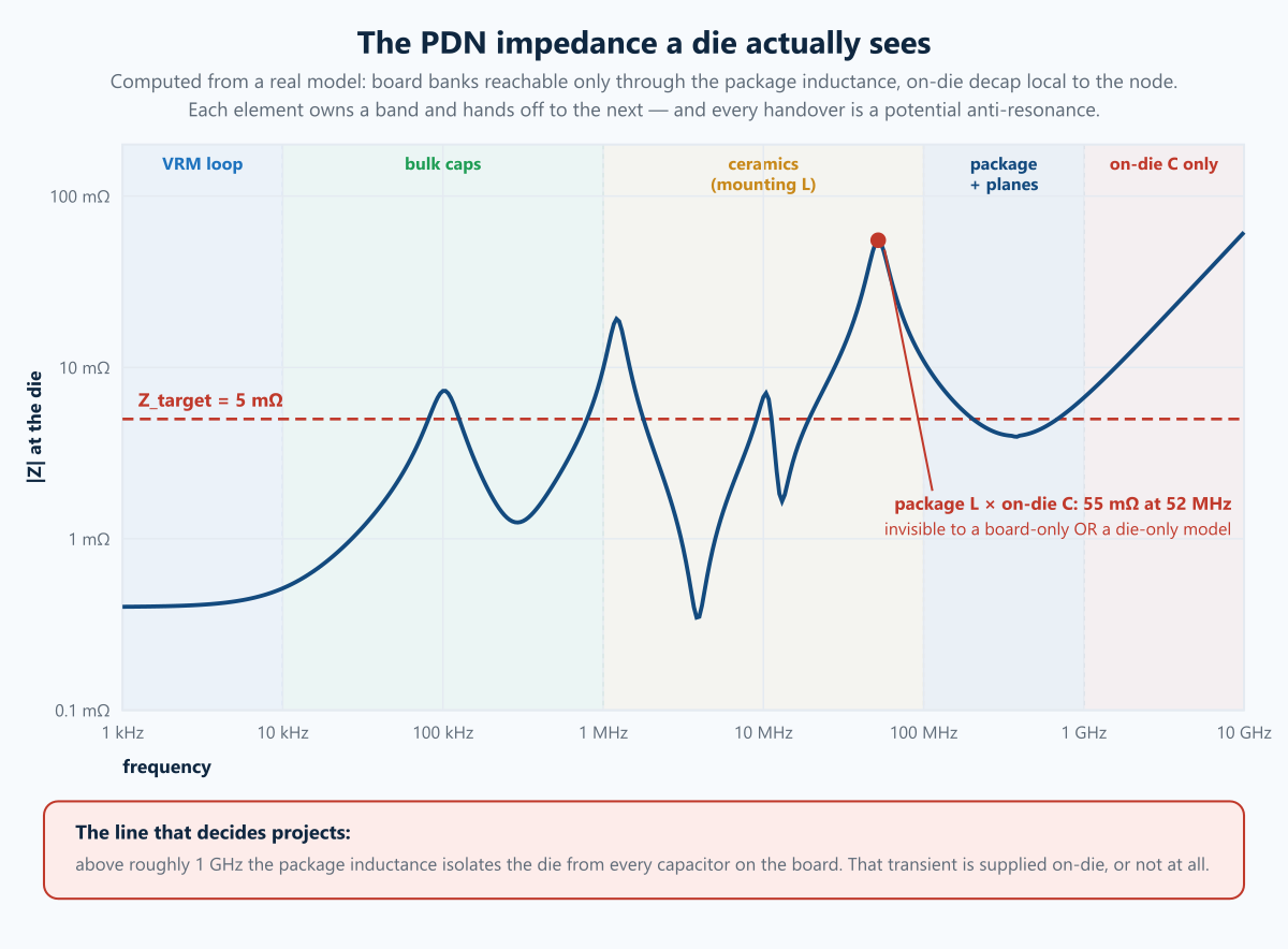
The PDN is a chain of parallel networks, each effective over a limited band, each handing off to the next. This is the single most useful mental model in power integrity:
| Band | Who supplies the current | Limited by |
|---|---|---|
| DC – ~10 kHz | The VRM’s control loop | Loop bandwidth, sense accuracy, plane R |
| ~10 kHz – 1 MHz | Bulk electrolytic / polymer capacitors | ESR, ESL, and their own SRF |
| ~1 MHz – 100 MHz | Ceramic decoupling on the board | Mounting inductance, not the capacitance |
| ~100 MHz – 1 GHz | Package capacitance and plane-pair capacitance | Package inductance, cavity modes |
| Above ~1 GHz | On-die capacitance only | Nothing on the board can reach this far |
That last row is the one that decides projects. Above roughly a gigahertz, the inductance between the die and anything on the board is too large for board components to respond. The transient is supplied by on-die decoupling capacitance and by the intrinsic capacitance of the power grid, or it is not supplied at all. You cannot fix a 1 GHz PDN problem on the PCB. Knowing that early changes which problems you accept and which you escalate to the silicon vendor.
8. Capacitors are inductors above their self-resonance
A real capacitor is C in series with ESR and ESL. It is capacitive below its self-resonant frequency, resistive at it, and inductive above it:
| Part + mounting | SRF |
|---|---|
| 100 µF bulk + 5 nH | 0.23 MHz |
| 1 µF + 1 nH | 5.03 MHz |
| 100 nF + 0.7 nH | 19.0 MHz |
| 10 nF + 0.5 nH | 71.2 MHz |
| 1 nF + 0.4 nH | 251.6 MHz |
Note what dominates. The difference between a 100 nF and a 10 nF part is one decade of capacitance, but their SRFs differ by less than a factor of four — because the loop inductance barely changed. Above a few tens of MHz, the value printed on the capacitor is nearly irrelevant; the mounting geometry is everything.
Mounting inductance, in the order that matters:
- Via length from the pad to the plane pair. This dominates. A capacitor on the top layer feeding planes 1.2 mm down has an unavoidable loop that no layout cleverness removes. Putting the plane pair close to the surface is worth more than any number of parts.
- Pad and fanout geometry. Via-in-pad beats a short trace stub, which beats a long one. Two vias per terminal roughly halves the inductance.
- Via spacing and orientation. Bringing the power and ground vias close together shrinks the loop area; interdigitating or using reverse-geometry parts helps.
- The package’s own ESL. Smaller case sizes have lower ESL — one reason 0402 and 0201 parts persist in decoupling roles where their capacitance alone would not justify them.
To make this concrete: 100 pH — an optimistic mounting inductance — is 628 mΩ at 1 GHz. Against a 2 mΩ target, one capacitor at 1 GHz is contributing three hundred times the allowed impedance. Hundreds in parallel bring that down proportionally, which is exactly why boards carry hundreds of decoupling capacitors, and also exactly why that strategy runs out.
9. Anti-resonance is the thing that actually bites
Put two capacitors with different SRFs in parallel. Between their resonances, one is already inductive and the other is still capacitive — and a parallel L-C is a parallel resonance, which is an impedance peak. Adding a capacitor to fix an impedance problem can therefore create a worse one at a nearby frequency.
This is the classic failure of the “one decade per capacitor value” recipe: a neat geometric ladder of 10 µF / 1 µF / 100 nF / 10 nF / 1 nF produces a neat ladder of anti-resonant peaks between them. Modern practice runs fewer distinct values with more parts each, chosen so the individual curves overlap rather than interleave, and accepts a slightly higher floor in exchange for no peaks. ESR is your friend here: a little series resistance damps the anti-resonance. Capacitors that are “too good” — very low ESR — make sharper peaks.
The decoupling impedance plot tool on the site plots a candidate network so you can see the peaks before you commit a BOM.
10. Plane cavities are resonators
A power-ground plane pair is a parallel-plate waveguide. Above the frequency where its dimensions approach a half wavelength, it has modes:
| Plane size ( = 4.2) | TM₁₀ | TM₀₁ | TM₁₁ |
|---|---|---|---|
| 200 × 150 mm | 366 MHz | 488 MHz | 610 MHz |
| 100 × 80 mm | 731 MHz | 914 MHz | 1171 MHz |
| 50 × 40 mm | 1463 MHz | 1829 MHz | 2342 MHz |
At a resonance, the impedance seen at some locations on the plane is high, and — worse — the cavity radiates from the board edges. The mitigations are: keep the plane pair thin (which raises both the interplane capacitance and the damping), place decoupling to damp the modes rather than in a decorative grid, and add edge termination or stitching where the mode structure demands it. A 2.5D solver finds these directly; this is one of the questions SIwave and PowerSI exist to answer.
Thin dielectric also buys real capacitance:
A 100 × 80 mm plane pair separated by 100 µm of = 4.2 laminate is 2.98 nF; halve the separation to 50 µm and it is 5.95 nF. That is a genuinely useful high-frequency capacitor with essentially zero mounting inductance, distributed exactly where it is needed — which is why “bury the plane pair close together, near the surface” is such a high-leverage stackup decision.
11. di/dt: where the real damage happens
Everything above is a frequency-domain view. The time-domain view is starker:
| Loop inductance | Current step | In | Voltage droop |
|---|---|---|---|
| 100 pH | 1 A | 100 ps | 1000 mV |
| 50 pH | 5 A | 200 ps | 1250 mV |
| 20 pH | 20 A | 500 ps | 800 mV |
| 1 nH | 10 A | 1 ns | 10 000 mV |
These numbers are not survivable on a 0.8 V rail, and that is the lesson. A fast current step cannot be supplied through any inductance a board can offer. The last row is deliberately absurd: it shows that if a 10 A, 1 ns step really had to come through 1 nH, the rail would collapse entirely. It does not, because on-die capacitance supplies it locally and the board only ever sees the slower envelope.
The real events that generate this:
- Clock gating and power gating. A block waking up is a current step with a very fast edge — and the inrush to recharge a gated domain’s own decoupling can exceed the block’s steady operating current. Well-designed power switches ramp deliberately in stages for exactly this reason.
- Workload transitions. An idle-to-full transition on a CPU or an AI accelerator: tens of amps in microseconds, which lands in the bulk-capacitor and VRM-loop bands.
- Simultaneous switching output (SSO). Many I/O drivers switching together, pulling through the shared package/board inductance. The resulting rail collapse appears as ground bounce and as timing pushout on the very signals that caused it.
- Resonant excitation. A periodic workload whose repetition rate lands on a PDN anti-resonance. This is the nastiest class, because the board passes every step-response test and then fails on one specific piece of firmware.
The first-order defences are, in order: reduce the inductance (stackup, mounting, package), add local capacitance as close to the die as the physics allows, damp the resonances, and — if all else fails — slow the edge. Slowing the edge is often the cheapest real fix and the one engineers reach for last.
Part III — On the chip
Board PDN work stops at the package balls. Inside, the same physics runs with different numbers and different tools.
The on-die power grid is a dense mesh of metal in the upper layers. It is resistive (hundreds of squares of thin metal), and it is where the last, largest share of the IR budget is spent. A rail that arrives at the bump within 3% can easily lose another 3–5% getting to the far corner of a large die.
Static IR and electromigration signoff is run in Ansys RedHawk-SC / Totem (analog) or Cadence Voltus, against the extracted grid and a per-instance power model. Outputs are a per-instance voltage map — feeding back into timing signoff, because a cell at reduced voltage is a slower cell — and current-density checks against the foundry’s EM rules for each metal layer.
Dynamic voltage drop is the on-die equivalent of di/dt: a vectorless or vector-driven analysis of switching activity against the grid plus on-die decoupling. The result decides how much on-die decap to spend area on, where to put it, and whether the clock architecture needs to stagger.
On-die decoupling is expensive in area and it leaks, so it is budgeted rather than sprinkled: MOS capacitors in the gaps of the standard-cell fabric, deliberate decap cells, and in advanced processes deep-trench or MIM capacitors. The trade against leakage power is a real design decision, not a formality.
The package sits between and is nobody’s default responsibility, which is why it is so often the problem. Bumps, redistribution, substrate planes, vias and balls each contribute inductance in the 10–100 pH class — precisely the range that governs the 100 MHz–1 GHz band where neither board nor die is in control.
Chip-package-board co-analysis
The three domains resonate with each other. The classic pathology is a peak formed between package inductance and on-die capacitance, typically in the 50–200 MHz range, that neither a board-only nor a die-only analysis can see, because each one terminates its model at the boundary where the other’s contribution lives.
Doing it properly means extracting each domain with the right tool — board in 2.5D (SIwave/PowerSI), package in 2.5D or 3D, die as a grid model plus its decap — and solving them as one network. It is more work than it sounds and it is the only way to find that class of resonance before silicon.
The tools
| Tool | Domain | What it is for |
|---|---|---|
| Ansys SIwave | Board/package 2.5D | DC IR, PDN impedance (Z-parameters), plane resonance, near-field EMI; the general-purpose PI tool |
| Cadence Sigrity PowerDC | Board/package DC | Electrothermal DC IR with coupled thermal iteration |
| Cadence Sigrity PowerSI / OptimizePI | Board/package AC | PDN impedance extraction and decap optimisation |
| Siemens HyperLynx PI | Board | Fast DC drop and decoupling analysis inside the Xpedition/PADS flow |
| Ansys Q3D Extractor | 3D quasi-static | The right tier for most PDN inductance questions — mounting, spreading, package — because those are extractions, not wave problems |
| Ansys Clarity / HFSS | 3D full-wave | Package and connector-level PDN structures where 2.5D assumptions break, and anything resonant |
| HSPICE / Spectre | Circuit | Transient PDN response with a real VRM model and a real current profile |
| Ansys RedHawk-SC / Totem | On-die | Static and dynamic IR, EM signoff |
| Cadence Voltus | On-die | Static and dynamic IR, EM signoff |
| Ansys Icepak / thermal solvers | Thermal | The other half of any honest DC analysis |
The on-die rows above have their own selection table in part one’s chip-side tool map, which covers extraction, on-die EM, package tiering and IR/EM signoff in one place.
A note on flow: DC and AC PI are usually the same model exercised two ways, so the effort that goes into a clean board extraction — correct stackup, correct material properties, correct sink definitions — pays for both. Set the model up once, properly.
Measuring a PDN, and why it is harder than it looks
You cannot measure a 1 mΩ impedance with an ordinary probe. The probe’s own ground lead is tens of nanohenries; the measurement is of the probe.
The two-port shunt-through method is the standard technique. Drive the rail from VNA port 1, receive on port 2, both connected at the same physical point, and compute:
for low impedances. Because the receiving port measures the voltage across the DUT rather than through the driving path, the technique remains accurate down to sub-milliohm levels. Two practical requirements dominate:
- Break the ground loop. The cable shields form a low-impedance path in parallel with the DUT, and at low frequency they dominate the reading. A common-mode transformer/isolator on one port, or a semi-rigid isolation, is mandatory — without it, everything below about 1 MHz is wrong and looks plausible.
- Land on a real four-point connection. Two separate probe points at the DUT, so the driving current does not flow through the sensing path. Designing a proper PDN measurement pad into the board costs nothing and is the difference between a usable measurement and an afternoon of arguing.
Other bench techniques worth having:
- VRM step-response test. An electronic load or a FET-switched resistor generating a controlled current step, with the rail observed on a wide-bandwidth scope AC-coupled through a low-inductance probe. This is the direct measurement of the thing you actually care about.
- Near-field probing. An H-field loop over the board finds where the switching currents actually flow and which cavities are ringing. Cheap, fast, and unreasonably informative.
- Thermal imaging under DC load. The static analysis’s ground truth: hot spots are current crowding, and they show up as the IR simulation’s current-density plot if the model is right.
Best practices
Static
- Budget the whole path explicitly — VRM setpoint, sense error, board, package, die — and check that the sum fits inside the rail tolerance at maximum temperature.
- Use planes for high-current rails; use remote sense where the drop is unavoidable.
- Distribute vias across the current front; count them and check per-via current.
- Analyse DC with thermal coupling for anything above a couple of amps.
- Size to IPC-2152, not the older charts, and derate for internal layers and enclosure temperature.
- Check current density at necks, not just average density.
Dynamic
- Compute for every rail, then treat it as a screen and convolve the real current profile for the rails that matter.
- Get the plane pair thin and near the surface — it is the highest-leverage stackup decision in PI.
- Optimise capacitor mounting, then capacitor count, then capacitor value, in that order.
- Use fewer distinct values with overlapping curves; do not build a geometric ladder.
- Do not chase the lowest possible ESR. Some damping prevents the peaks.
- Check for anti-resonances explicitly — plot the network impedance, look for peaks, and verify no workload frequency lands on one.
- Simulate plane cavity modes on any board with large planes and fast edges.
- Ask the silicon vendor for a current profile and an on-die capacitance figure. If they will not give you either, your PDN model has a hole in it exactly where the highest frequencies live, and you should say so in writing.
- Design a PDN measurement point into the board.
The pitfalls that cost the most time
- Lumping a BGA’s current draw at a single node.
- Running DC analysis at room temperature.
- Adding capacitors to fix an impedance peak, and creating a new one.
- Treating the capacitor’s printed value as its high-frequency behaviour.
- Modelling the board and stopping at the balls — the package/die resonance is invisible from there.
- Measuring PDN impedance without breaking the cable ground loop.
- Expecting board decoupling to help above ~1 GHz.
- Ignoring the VRM’s control-loop stability, which sets everything below ~10 kHz and can itself peak.
Run the numbers yourself
- PDN target impedance — from rail voltage, ripple and transient current
- Decoupling impedance plot — plot a candidate capacitor network and find the anti-resonances
- Thermal via calculator — via arrays for heat, the other half of the current-carrying question
- Buck converter calculator — inductor and output-capacitor sizing for the VRM feeding all of this
- Board FIT calculator — reliability roll-up when the rail is part of a safety-relevant function
The full set is at circuit-design.space/tools.
Where we fit
Power integrity is core work for us, alongside schematic capture, layout and signal integrity — in Cadence Allegro, Altium Designer, Ansys SIwave and Siemens HyperLynx. On programmes with a functional-safety requirement we also produce the FMEDA and FMEA evidence, and power delivery is one of the places where that pairing matters: wear-out mechanisms like electromigration and capacitor ageing are quantitative reliability inputs, not footnotes.
If you have a rail that droops, a board that only fails under one firmware load, or a stackup decision you would rather make with an impedance plot than with precedent, that is the conversation we like having.
Glossary
Anti-resonance — The impedance peak formed when a capacitive branch and an inductive branch resonate in parallel; the main hazard when combining decoupling capacitor values.
Black’s equation — ; the wear-out model for electromigration.
Bulk capacitance — Large electrolytic, tantalum or polymer capacitors covering roughly 10 kHz–1 MHz: the band between where the regulator’s control loop gives up and where the ceramics take over. Usually chosen on ESR as much as capacitance, because a little ESR damps the anti-resonance with the ceramics rather than sharpening it.
Decap — Decoupling capacitance, on board or on die. The board kind supplies charge over nanoseconds to microseconds; the on-die kind is the only thing fast enough for the first picoseconds, because the package inductance isolates the die from everything outside it.
DvD (dynamic voltage drop) — On-die rail droop caused by switching activity, as distinct from static IR. The one that actually closes or fails timing, because it is local and instantaneous: an average rail can be healthy while one corner of one block browns out during a simultaneous clock edge.
Electromigration (EM) — Current-driven migration of metal atoms that thins a conductor until it opens. Governed by Black’s equation, so it is quadratic in current density and exponential in temperature. It is a wear-out mechanism, which makes it a reliability-lifetime question rather than a does-it-work-today one.
ESL / ESR — Equivalent Series Inductance and Resistance: the parasitics that define what a real capacitor does away from DC. ESR sets the floor of the impedance dip at resonance; ESL sets everything above it. On a modern MLCC both are dominated by how it is mounted, not by the part.
Ground bounce — The local rise of a reference node when return current flows through the return path’s inductance, . The reason “ground” is a net name rather than a voltage, and the reason a return path discontinuity matters as much as the signal path.
IPC-2152 — The measurement-based standard for PCB conductor current-carrying capacity. It supersedes the old IPC-2221 charts, which were conservative in some cases and optimistic in others because they came from 1950s data on very different boards. Use it for actual temperature-rise numbers rather than folklore.
IR drop — Static voltage loss along a conductor, straight from Ohm’s law. Simple, easy to compute, and routinely the smaller half of the problem — the dynamic term is what usually breaks things, but IR eats the margin the dynamic term then has to fit inside.
Mounting inductance — The loop inductance from a capacitor’s terminals out through its pads, its vias and the plane pair. Above a few tens of megahertz it, not the capacitance, sets the impedance — so capacitor placement and via count change the PDN far more than the printed capacitance value does. Two vias per pad instead of one is a real improvement.
PDN — Power Delivery Network: everything between the regulator and the transistor, seen as one impedance-versus-frequency curve. The useful mental model is a relay team, each stage covering a frequency band and handing over to the next.
Plane cavity resonance — The parallel-plate waveguide modes of a power/ground plane pair, set by the board’s lateral dimensions. Shows as impedance peaks at specific frequencies, and the modes are spatial — the impedance depends on where on the board you look, so a single lumped PDN model cannot represent them.
Remote sense — Feeding the regulator’s feedback from the load rather than from its own output, so the control loop corrects for the drop in between. Free accuracy at DC and low frequency, and worth the two extra traces on any high-current rail.
Shunt-through measurement — The two-port VNA technique for measuring milliohm impedances, because a one-port reflection measurement has no resolution down there. Needs a ground-loop isolator (or a semi-rigid/balun arrangement) to be valid at low frequency, and omitting it is the classic way to measure your own cable braid instead of the PDN.
Spreading inductance / resistance — The contribution of current spreading laterally through a plane, distinct from the via and trace terms. It is why a capacitor’s effectiveness falls with distance from the load even on a solid plane, and why “there is a plane, it is fine” is not an argument above a few tens of megahertz.
SRF — Self-Resonant Frequency, . Below it a capacitor is capacitive; above it, inductive. A 100 nF 0402 is an inductor by 20–30 MHz, which is why decoupling uses a spread of values and why simply adding more of the same part stops helping.
SSO / SSN — Simultaneous Switching Output / Noise: many drivers switching together through a shared return inductance, so the noise scales with how many bits change at once. The reason bus encoding and staggered output timing exist, and the reason a memory interface’s worst case is a data pattern rather than a single edge.
Target impedance () — : the flat-impedance design heuristic. Useful for sizing, and a heuristic rather than a law — a real load’s current spectrum is not flat, so a PDN that meets target everywhere may be over-designed at some frequencies and under-designed at the one that matters.
VRM — Voltage Regulator Module. Owns the PDN below roughly 10 kHz through its control loop, and is an active element: its loop bandwidth, not its output capacitance, decides where it hands over to the bulk capacitors, and a loop that peaks can add an impedance bump of its own.
Further reading — reference books
Book links below are Amazon affiliate links: if you buy through one we earn a small commission at no extra cost to you. It does not influence what is recommended — the same books were on this list before the links were.
- Eric Bogatin, Signal and Power Integrity — Simplified.
- Larry Smith & Eric Bogatin, Principles of Power Integrity for PDN Design — Simplified. The definitive treatment; the shunt-through measurement discussion alone justifies it.
- Madhavan Swaminathan & A. Ege Engin, Power Integrity Modeling and Design for Semiconductors and Systems.
- Henry Ott, Electromagnetic Compatibility Engineering.
- Mark Montrose, EMC and the Printed Circuit Board.
- IPC-2152, Standard for Determining Current-Carrying Capacity in Printed Board Design.
- JEDEC JEP122, on failure mechanisms and models for semiconductor devices (including electromigration).
Have a rail that will not hold, or a PDN you would rather design than debug? That’s what we do. Reach us at circuit-design.space.
circuit-design.space · +1-971-357-1400 · anovickis@circuit-design.space