Part of the RF chain series — a page per block. Neighbours: the filter in front of it, and the mixer behind.
The RF chain, block by block —Antenna · Filter · LNA · Mixer · LO · IF & ADC · PA · Isolator · Coupler · Overview
The LNA is the first active thing a received signal meets, and that position gives it a disproportionate say in what the whole receiver can hear. Everything downstream adds noise too, but it adds it to a signal the LNA has already amplified — so the LNA’s own noise is the only noise that gets the full benefit of the chain’s gain.
1. What the position buys you
Noise cascades by the Friis formula:
Worked, for a realistic front end:
| Stage | NF | Gain | (linear) | Contribution to |
|---|---|---|---|---|
| LNA | 1.2 dB | +18 dB | 1.318 | 1.318 |
| Mixer | 8.0 dB | −7 dB | 6.310 | 0.084 |
| IF amp | 4.0 dB | +25 dB | 2.512 | 0.120 |
| F = 1.523 | NF = 1.83 dB |
Two lessons sit in that table, and the second is the one people miss.
The first stage dominates — the LNA contributes 1.318 of the 1.523 total. An 8 dB mixer sitting behind 18 dB of gain costs almost nothing.
But it does not dominate completely. The later stages still add 0.20, turning a 1.2 dB LNA into a 1.83 dB system. Anyone who says “the LNA sets the noise figure” and stops has under-predicted by six tenths of a dB, which on a link budget is real range.
The corollary is the design rule: gain in the first stage suppresses everything behind it, so more LNA gain is always better for noise — and always worse for linearity, because everything downstream now sees a bigger signal. That tension is the whole of LNA design.
And the noise floor it is working against:
| Bandwidth | Thermal floor | With NF 1.83 dB |
|---|---|---|
| 1 MHz | −114.0 dBm | −112.2 dBm |
| 20 MHz | −101.0 dBm | −99.2 dBm |
| 100 MHz | −94.0 dBm | −92.2 dBm |
Two other ways of writing the same fact are worth carrying, because different parts of a system specification use different ones.
Noise temperature replaces the ratio with an equivalent input temperature:
so a 1.2 dB LNA is a 92 K amplifier. Below about 1 dB the decibel scale compresses badly — 0.5 dB and 0.3 dB are 35 K and 21 K, a 40% difference the dB number hides — which is why radio astronomy and satellite ground stations specify and everyone else specifies NF. If you are ever asked to improve a 0.4 dB front end, translate to kelvin first; the job is usually larger than it sounds.
Sensitivity is the number a system engineer actually asks for:
For a 20 MHz channel needing 10 dB SNR at the demodulator, the 1.83 dB chain above gives dBm. Improve the noise figure by 0.6 dB and you gain 0.6 dB of link budget — in free space more range, and indoors where path loss runs closer to , about 4%. That conversion is how you argue for an expensive LNA: not “0.6 dB better”, but “7% more range”, or “one fewer base station”.
2. The specification that actually matters
| Parameter | What it means | Typical |
|---|---|---|
| Noise figure | SNR degradation through the stage | 0.5–2 dB below 6 GHz; 2–4 dB at mmWave |
| Gain | 12–20 dB; more starves linearity | |
| IIP3 | Input third-order intercept | −10 to +5 dBm typical |
| P1dB | Input compression point | usually ~10 dB below IIP3 |
| / | Input and output match | −10 dB minimum, −15 dB preferred |
| Stability (K, |Δ|) | Will it oscillate | , everywhere, not just in band |
| Supply and current | Efficiency, and how hot it runs | sets the noise/linearity ceiling |
3. The thing that makes LNA design different
The noise match is not the power match. The source impedance that gives minimum noise figure, , is generally not the conjugate match that gives maximum gain. They are different points on the Smith chart, and every LNA design is a decision about where to sit between them.
Noise figure as a function of source admittance:
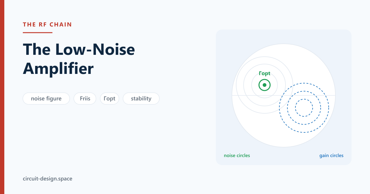
The four numbers on the right — , , and the magnitude and angle of — are the noise parameters, and a device datasheet that omits them cannot be designed with. Plotting constant-noise-figure circles and constant-gain circles together on the Smith chart shows the trade directly, and choosing a point between them is the design.
is the sensitivity: a device with small tolerates being away from cheaply, and one with large punishes it.
Constant-noise circles, explicitly
The locus of source reflection coefficients giving a particular noise figure is a circle on the chart. Define the noise parameter
and the circle has centre and radius
At , and the circle collapses to the point ; as rises the circles grow and drift toward the origin. Overlay the available-gain circles on the same chart and the design reduces to choosing a point on the best compromise contour — which is exactly what a simulator is doing when you ask it for a noise-circle plot. Doing it once by hand is worth the hour, because it makes visible how flat the trade usually is: for a good device, the 0.1 dB circle is often large enough to contain a perfectly respectable match.
What the noise match costs in gain
Sitting at rather than at the simultaneous conjugate match costs gain, and the amount is worth computing rather than guessing. Available gain as a function of the source:
For a typical low-noise pHEMT at 2 GHz the noise match costs 1–2 dB of available gain against the power match. In the first stage that is nearly always the right trade — Friis only needs the gain to be large enough to suppress stage two. In the second stage it is the wrong one, and designing both stages for is a common and expensive habit.
Note also that depends on alone, not on the load. That is why the available-gain design flow, not the transducer-gain one, is the right frame for an LNA: you choose the source for noise, read off the gain it permits, then conjugate-match the output to collect it.
The number to use when the stage will be cascaded with itself
If several identical stages will follow one another — a distributed antenna system, a repeater, a long IF strip — neither nor alone is the right figure of merit. Noise measure is:
the noise figure of an infinite cascade of the stage. Minimising rather than is what you want there, and it will pick a different source impedance: a little more gain in exchange for a little more noise.
4. Topologies
Inductively degenerated common-source is the workhorse in CMOS and the reason LNA design is tractable at all. A small inductor in the source produces a real input impedance without adding a physical resistor — and a resistor would add its own thermal noise. Neglecting :
The last term is purely real and contains no resistor — it is a resistance manufactured out of a reactance and a transconductance, and it therefore contributes no thermal noise of its own. Writing , it is simply , so
for a 100 GHz- device into 50 Ω. Eighty picohenries is a bond wire, or a couple of hundred microns of on-chip trace — which is the practical consequence: the degeneration inductor is small enough that the layout parasitics are the design, and the value you simulate has to come from an EM extraction rather than a schematic symbol. then resonates the reactive part at band centre, .
The useful accident of this topology is that for a MOSFET the resulting lands close to — a simultaneous noise and power match — which is why it is everywhere. The accident is only approximate, and forcing it exactly is what the power-constrained variants below are for.
Cascode stacks a common-gate device on top. It raises output impedance, improves reverse isolation (smaller , so better stability — look again at the expression and note in the denominator), and reduces the Miller effect at the cost of voltage headroom. That last cost is why cascodes get harder at each process node: the supply falls and the threshold does not.
Common-gate gives a wideband input match set by — easy and broadband, and independent of , so it does not narrow. The price is a noise-figure floor: matching fixes , and fixing fixes the channel noise relative to the source, giving , which in practice is hard to push below about 3 dB.
Distributed / travelling-wave absorbs device capacitance into an artificial transmission line, so the thing that limits bandwidth becomes part of the matching structure. Multi-octave bandwidth, at the cost of area, current, and a noise figure worse than a tuned stage.
Noise-cancelling topologies sense the matching device’s noise at two points where it appears with opposite sign and subtract it, breaking the usual link between input match and noise figure entirely. This is what makes a wideband CMOS receiver with a resistive-feedback input possible at all, and it is the standard trick in modern SDR front ends.
Resistive feedback (shunt-series) deserves mention as the pragmatic wideband answer: flat gain, good match over a decade, easy to build — and a noise figure typically 1–2 dB worse than a tuned design, because the feedback resistor is a real resistor.
5. Bias: the current density nobody tells you about
Ask what current to run an LNA at and the datasheet gives you one operating point. The underlying rule is more portable, and it is a current density, not a current:
| Density (CMOS) | What happens there |
|---|---|
| mA/µm of gate width | minimum noise figure |
| mA/µm | peak , peak gain |
| below mA/µm | collapses, NF rises steeply |
The optimum-noise density is remarkably stable across nodes, which makes it a genuinely useful design rule: pick the density from the table, then pick the width from the current you can afford. Doubling the width at fixed density doubles the current and roughly halves and the optimum source resistance — so width is the knob that walks toward 50 Ω, and current is what you pay for the walk.
For discrete bipolar and SiGe devices the equivalent statement is a collector current. has a shallow minimum at a few milliamps and rises on both sides, because base shot noise grows with while the contribution of base resistance falls with it. The datasheet plot of against is the whole story and is nearly always printed — read it before choosing a bias resistor, not after.
When the current is fixed. If the battery budget sets the current, you cannot generally have the noise optimum and the input match from the same device size. The standard resolution, PCSNIM (power-constrained simultaneous noise and input match), adds an explicit capacitor across : it moves without changing the bias, at a cost in and a little noise. That is the capacitor on a handset LNA schematic that looks as though it does nothing.
6. Stability, which comes before everything
An amplifier that oscillates is not an amplifier. Rollett:
with unconditional stability requiring and . Most useful devices are only conditionally stable where they have gain, which means there exist source and load impedances that will oscillate, and you must know where they are.
Most LNA oscillations are out of band and low frequency, in the bias network, at a frequency nobody simulated. Device gain rises as frequency falls, so a transistor that is marginal at 5 GHz has enormous gain at 50 MHz — and the bias inductor that looks like an RF choke in band is a resonator somewhere else. Simulate stability from DC to beyond , not across the band of interest.
Two refinements are worth having beyond the pass/fail of :
is the better single number. Rollett’s needs an auxiliary condition (, or equivalently ) and is therefore not, by itself, a test. The geometric stability factor is:
is necessary and sufficient for unconditional stability, and — this is the part that makes it useful — is the distance from the centre of the Smith chart to the nearest unstable load, so larger genuinely means “more stable”. tells you nothing about margin; does.
Where the stability circles are matters more than whether they exist. A conditionally stable device is perfectly usable if the unstable region sits somewhere your source and load can never go. Plot the input and output stability circles across the full frequency sweep and ask a different question: not “is it unconditionally stable” but “can the antenna, the filter in front, or the next stage’s input present an impedance inside that circle at any frequency, including with a cable of unknown length attached”. A receive LNA whose input sees a disconnected antenna sees at every phase, which sweeps the entire edge of the chart — so for that case only unconditional stability will do.
The usual stabilising moves, in rough order of noise cost: a series resistor in the drain bias feed (cheap, kills low-frequency gain where the trouble is, costs nothing in band); a small shunt RC at the output; resistive loading at the input (effective, and it adds its noise directly to — a last resort on a first stage).
7. A design method that works
- Budget the chain first. Decide the system NF and the linearity target, then allocate. The RF chain overview covers this.
- Pick a device on at your frequency and the current you can afford. Check the noise parameters exist.
- Check stability across the full frequency range, before designing any matching. Stabilise with resistive loading or a lossy bias feed if needed, and re-check the noise cost.
- Plot noise and gain circles together; choose the source impedance.
- Design the input match toward , the output match for gain and .
- Field-solve the passives. Above a few GHz the matching structures, pads and vias are distributed — see which solver to use.
- Simulate linearity with a two-tone harmonic-balance sweep.
- Re-check stability with the real matching networks and the real bias network in place.
- Measure, and reconcile.
8. Measuring noise figure without fooling yourself
Y-factor is the standard method: a calibrated noise source is switched between hot and cold, and the output power ratio of the two states gives the noise figure directly:
where ENR is the source’s excess noise ratio. The arithmetic explains the method’s own weakness: a low-noise DUT gives a large , and then depends on the difference, so a small error in the measured ratio becomes a large error in . At 0.5 dB noise figure, 0.1 dB of power-measurement error is roughly 0.1 dB of noise figure error — the method has no margin left.
The traps:
- Loss ahead of the DUT adds directly to the measured NF. A 0.5 dB cable is 0.5 dB of noise figure. Calibrate it out, or measure it and subtract.
- ENR calibration drifts. The noise source’s excess-noise ratio is frequency-dependent and its calibration expires.
- A mismatched DUT breaks the assumption the method rests on. Poor makes the measurement unreliable, not just the amplifier.
- Cold-source / vector-corrected methods on a modern VNA are more accurate and correct for mismatch, at the cost of a more involved calibration.
Below about 1 dB, noise-figure measurement is genuinely difficult and the number deserves scepticism — including your own.
9. A worked front-end budget, with the losses included
The §1 table was the textbook version: LNA, mixer, IF amp. A real receiver has a cable, a pre-select filter and a switch in front of the LNA, and including them changes the conclusion enough to be worth doing once in full. A 2.4 GHz receiver:
| # | Stage | NF (dB) | Gain (dB) | IIP3 (dBm) |
|---|---|---|---|---|
| 1 | Antenna cable + connector | 0.8 | −0.8 | — |
| 2 | Pre-select filter | 1.5 | −1.5 | — |
| 3 | T/R switch | 0.6 | −0.6 | +45 |
| 4 | LNA | 1.2 | +18.0 | −8 |
| 5 | Image filter | 2.0 | −2.0 | — |
| 6 | Mixer | 8.0 | −7.0 | +5 |
| 7 | IF amplifier | 4.0 | +25.0 | +10 |
Cascading: total gain 31.1 dB, NF 5.08 dB, input-referred IIP3 −10.0 dBm (OIP3 +21.1 dBm). And the share of the excess noise factor , which is where the lesson is:
| Stage | Share of |
|---|---|
| Antenna cable + connector | 9.1% |
| Pre-select filter | 22.3% |
| T/R switch | 11.3% |
| LNA | 28.0% |
| Image filter | 0.8% |
| Mixer | 11.7% |
| IF amplifier | 16.7% |
The 1.2 dB LNA produced a 5.08 dB receiver, and it is responsible for barely a quarter of the damage. The 2.9 dB of passive loss ahead of it contributes 42.7% between them, and every one of those decibels was bought with a connector, a cable and a filter that somebody chose without doing this sum. Before optimising the LNA, optimise what is in front of it: a lower-loss filter, a shorter cable, or moving the LNA to the antenna is worth more than an exotic device.
The ordering matters as much as the parts. Move the LNA behind the image filter — the same seven components, one swap — and the chain becomes 6.73 dB, 1.65 dB worse, for no change in bill of materials and almost no change in linearity (IIP3 −9.5 dBm). That is the loss-before-gain rule with a number attached.
And the linearity side of the same argument: the LNA’s 18 dB of gain is what drags the chain’s referred IIP3 down to −10 dBm. Drop the LNA gain to 12 dB and the noise figure worsens by only a few tenths while the referred IIP3 improves by most of 6 dB. First-stage gain is the single control that trades the receiver’s noise floor against its blocking performance, and it should be set deliberately from the blocker spec, not taken from whatever the MMIC happens to have.
10. Example parts, with the reason you would choose each
Real devices, to make the trade concrete. Availability changes — check current stock and the current datasheet rather than trusting a table in a blog post — but the shape of the choice is stable.
Gain blocks and MMIC LNAs (a match already built in, which is most of the work):
| Part | Range | NF / gain | Why you would pick it |
|---|---|---|---|
| Mini-Circuits PSA4-5043+ | 0.05–4 GHz | ≈0.7 dB / ≈22 dB | E-pHEMT MMIC, 50 Ω in and out, the default “just make it work” part |
| Qorvo SPF5189Z | 0.05–4 GHz | ≈0.6 dB / ≈18 dB | very low NF for a matched MMIC; popular in GNSS and ADS-B front ends |
| MACOM MAAL-011078 | 0.7–6 GHz | ≈0.7 dB / ≈18 dB | wideband, covers cellular and both ISM bands in one part |
| Analog Devices HMC717A | 0.4–4 GHz | ≈0.9 dB / ≈16 dB | GaAs pHEMT MMIC with respectable OIP3 for its noise figure |
| Mini-Circuits ZX60-P33ULN+ | 0.05–3 GHz | ≈0.4 dB / ≈21 dB | connectorised — the fastest way to put a known-good LNA in a measurement |
Discrete transistors (more work, better noise figure, and you control the match):
| Part | Technology | Why you would pick it |
|---|---|---|
| Infineon BFP840ESD | SiGe:C, ≈ 68 GHz | around 0.65 dB at 1.8 GHz, and ESD-protected, which matters on an antenna port |
| NXP BFU730F | SiGe:C | wideband low-noise workhorse with published noise parameters |
| Broadcom ATF-54143 | E-pHEMT | the classic 2.4 GHz low-noise device; enormous body of published designs |
| Qorvo TQP3M9037 | GaAs pHEMT | low NF with high OIP3 — the combination that is hard to buy |
The selection question is almost never “which has the lowest “. It is: does the datasheet publish the four noise parameters at my frequency, can I present with the board I can afford, and does the part have enough OIP3 to survive the blockers my antenna will actually see? A device with 0.4 dB and no published is not designable, and a device with 0.6 dB and +30 dBm OIP3 will beat it in a real radio.
One practical note on ESD and survival. An LNA input is connected to an antenna, which is connected to the outside world. Transmit leakage from a nearby radio, static on a whip, and hot-plugging a cable all arrive at the gate of a device whose entire design brief was to be fragile and quiet. Either buy the ESD-protected variant or put a shunt inductor to ground at the input — it is a DC short and an RF open, it costs a fraction of a dB, and it is why so many production LNA front ends have an inductor that the schematic does not seem to need.
11. The pitfalls
- Declaring a device stable on the strength of an in-band .
- Using without its auxiliary condition, or reading as adequate margin.
- Designing the input for a power match and reporting the datasheet .
- Ignoring loss in front of the LNA: filter, cable and switch insertion loss is noise figure, one for one — and in the budget above it outweighed the LNA itself.
- Too much LNA gain, compressing the mixer behind it and wrecking the chain’s IIP3.
- Choosing a bias current from the “typical application” box rather than from the -versus-current curve.
- Bias networks omitted from the simulation, then oscillating in hardware.
- Simulating the degeneration and matching inductors as ideal components instead of extracting them.
- Measuring NF through a fixture that was never de-embedded.
- No ESD path at an input that is wired to an antenna.
Further reading
- Guillermo Gonzalez, Microwave Transistor Amplifiers: Analysis and Design. The noise circles, gain circles and stability circles in this post are all derived here, in full. If you own one amplifier book, own this one.
- Thomas Lee, The Design of CMOS Radio-Frequency Integrated Circuits. The inductively degenerated CMOS LNA, from the device physics up.
- Behzad Razavi, RF Microelectronics. The best treatment of noise-cancelling and wideband receiver front ends.
- David Pozar, Microwave Engineering. For the S-parameter and matching groundwork underneath all of it.
- Joel Dunsmore, Handbook of Microwave Component Measurements. The chapter on noise-figure measurement is the one to read before you dispute a supplier’s number — or defend your own.
The RF chain, block by block —Antenna · Filter · LNA · Mixer · LO · IF & ADC · PA · Isolator · Coupler · Overview
Glossary
Available gain () — Gain as a function of the source impedance alone, independent of the load. That independence is why the available-gain flow, not the transducer-gain one, is the right frame for an LNA: choose the source for noise, read off the gain it permits, then conjugate-match the output to collect it.
Cascode — A common-gate device stacked on a common-source one. Raises output impedance, shrinks and so improves stability, and reduces the Miller effect — at the cost of voltage headroom, which is why cascodes get harder at every node as the supply falls and the threshold does not.
Cold-source method — Vector-corrected noise-figure measurement on a VNA, which corrects for DUT mismatch instead of assuming it away. More accurate than Y-factor below about 1 dB, at the cost of a considerably more involved calibration.
ENR — Excess Noise Ratio: how much hotter than 290 K a calibrated noise source is when fired. Frequency-dependent, and its calibration expires — an out-of-date ENR table is a silent, systematic error in every noise figure the bench produces.
, , — The four noise parameters. is the best achievable noise figure, the source reflection coefficient that achieves it, and the sensitivity to being away from it. A datasheet that omits cannot be designed with, whatever it advertises.
Inductive degeneration — A small source inductor producing a real input impedance without a physical resistor, and therefore without the resistor’s noise. At 80 pH for a 100 GHz- device into 50 Ω it is a bond wire, which means the layout parasitics are the design.
Noise circles — Loci of constant noise figure on the source plane, shrinking onto as . Overlaid with gain circles they turn the LNA trade into a picture, and the useful thing they show is how flat it usually is.
Noise-cancelling — Topologies that sense the matching device’s noise where it appears with opposite sign and subtract it, breaking the link between input match and noise figure. What makes a wideband resistive-feedback CMOS front end viable at all.
Noise measure () — : the noise figure of an infinite cascade of the stage. The right figure of merit when several identical stages will follow one another, and it picks a different source impedance than minimising does.
Noise temperature () — , in kelvin. Below 1 dB the decibel scale compresses badly — 0.5 dB and 0.3 dB are 35 K and 21 K — so radio astronomy and satellite ground stations specify and everyone else specifies NF. Translate before agreeing to improve a 0.4 dB front end.
PCSNIM — Power-constrained simultaneous noise and input match: adding a capacitor across to move without changing the bias. The capacitor on a handset LNA schematic that appears to do nothing.
Sensitivity (MDS) — , in dBm. The number a system engineer actually asks for, and the right way to argue for a better LNA: 0.6 dB is not “0.6 dB better”, it is 7% more range in free space.
Stability factor () — The geometric criterion. is necessary and sufficient on its own, unlike , which needs an auxiliary condition — and is a distance to the nearest unstable load, so larger genuinely means more margin. tells you nothing about margin; does.
Stability circles — The boundary of source or load impedances that would oscillate. The useful question is not whether they exist but whether your circuit can reach inside one — and a receive LNA whose antenna can be disconnected sees every phase on the unit circle, so for that case only unconditional stability will do.
Related
- The RF chain overview — how the blocks fit together
- The filter in front of it — whose insertion loss is your noise figure
- The mixer behind it — usually the chain’s linearity bottleneck
- The Smith chart — where noise and gain circles get drawn
- S-parameters and Touchstone — the data you design from
Have a front end that does not meet its noise figure, or an amplifier that oscillates somewhere you did not simulate? That’s what we do. Reach us at circuit-design.space.
circuit-design.space · +1-971-357-1400 · anovickis@circuit-design.space