Third in a five-part series. Part one covered signal integrity — the channel, the connector, and which solver to reach for. Part two covered power integrity, from static IR drop to rapid di/dt. Parts four and five move inside the die: on-die signal integrity and silicon power usage.
The RF chain, block by block —Antenna · Filter · LNA · Mixer · LO · IF & ADC · PA · Isolator · Coupler · Overview
Signal integrity and RF are the same physics with different questions. SI asks did the bit survive. RF asks what is the power, the noise, the linearity, and what unwanted frequencies did I create along the way. The transmission-line theory is shared; almost nothing else is.
The other difference is cultural. In SI, a discontinuity is a defect to be removed. In RF, a discontinuity is a component — a stub, a coupled line, a resonator — deliberately placed because its reflection is the thing doing the work. That inversion is why an SI engineer’s instincts do not automatically transfer, and vice versa.
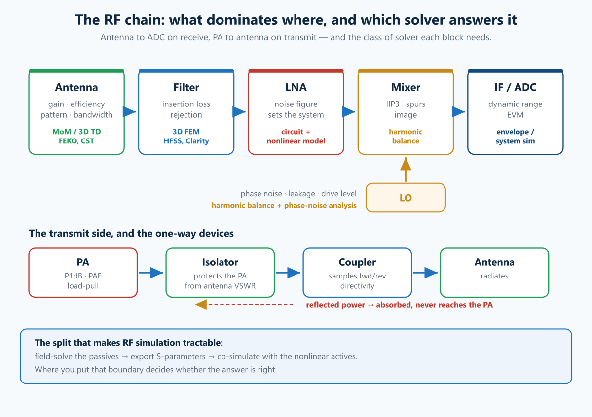
Here is the whole article in one picture: the chain, the figure of merit that dominates at each point, and the class of solver that answers it.
1. The common language: S-parameters
At microwave frequencies you cannot measure voltage and current at a plane — the probe is part of the circuit. So RF measures travelling waves instead, in a defined reference impedance, usually 50 Ω:
where are the incident waves and the reflected and transmitted ones. The four terms of a two-port:
| Term | Definition | Meaning |
|---|---|---|
| , port 2 matched | input reflection | |
| , port 2 matched | forward transmission — gain or insertion loss | |
| , port 1 matched | reverse transmission — isolation, and the route to instability | |
| , port 1 matched | output reflection |
Two companion posts go deeper on this: S-parameters and Touchstone files on what the data means and how the files are structured, and the Smith chart guide on reading reflection graphically.
Everything else is derived. Return loss is . Insertion loss is . VSWR follows from |Γ|. And the reflection table from part one applies unchanged:
| Load on 50 Ω | Γ | Return loss | VSWR | Power reflected |
|---|---|---|---|---|
| 55 Ω | 0.048 | 26.4 dB | 1.10 | 0.23% |
| 60 Ω | 0.091 | 20.8 dB | 1.20 | 0.83% |
| 75 Ω | 0.200 | 14.0 dB | 1.50 | 4.0% |
| 100 Ω | 0.333 | 9.5 dB | 2.00 | 11.1% |
Matching is the act of transforming a load to the reference impedance over a band. The tools are L-networks and pi/T-networks at lower frequencies, and distributed structures — quarter-wave transformers, stubs, coupled lines, tapers — as soon as a quarter wavelength is a manufacturable size:
| Frequency | (air) | (air) | in |
|---|---|---|---|
| 915 MHz | 327.6 mm | 81.9 mm | 40.0 mm |
| 2.45 GHz | 122.4 mm | 30.6 mm | 14.9 mm |
| 5.8 GHz | 51.7 mm | 12.9 mm | 6.3 mm |
| 28 GHz | 10.7 mm | 2.68 mm | 1.31 mm |
| 77 GHz | 3.89 mm | 0.97 mm | 0.47 mm |
Read the bottom two rows carefully. At 28 GHz a quarter-wave stub in laminate is 1.31 mm, and at 77 GHz it is 0.47 mm — comparable to the etch tolerance and the solder fillet. This is why millimetre-wave design is a manufacturing problem as much as an electrical one, and why 3D electromagnetic simulation of the as-fabricated geometry, including pads and transitions, stops being optional.
A quarter-wave transformer is inherently narrowband. Broadband matching costs sections (multi-section Chebyshev transformers, tapers), and is bounded by the Bode–Fano limit — for a given load Q, there is a hard trade between bandwidth and achievable match. You cannot match a high-Q load broadly, no matter how clever the network. Knowing that limit saves weeks.
2. Amplifiers
Gain
Several gains coexist and are routinely confused. is the transducer gain into a matched system — the one a VNA reports. Available gain and operating power gain assume conjugate matching at one port. Maximum available gain (MAG) is the best possible with both ports conjugately matched, and it only exists when the device is unconditionally stable. When it is not, the meaningful number is maximum stable gain (MSG), .
Stability — check it before anything else
An amplifier that oscillates is not an amplifier. The Rollett conditions:
Worked, so the numbers are concrete:
| | | | | | | Verdict | |—:|—:|—:|—:|—:|—:|—| | 0.7 | 0.03 | 3.0 | 0.5 | 1.820 | 0.260 | unconditionally stable | | 0.9 | 0.05 | 5.0 | 0.8 | −0.458 | 0.470 | potentially unstable |
The second row is an ordinary high-gain device, and it is what most useful transistors look like at the frequencies where they have gain. Potentially unstable does not mean unusable — it means there exist source and load impedances that will make it oscillate, and you must know where they are. Plot the stability circles on the Smith chart, keep the design impedances outside them, and remember that the impedance presented at frequencies outside your band — by the bias network, by a long DC feed, by the next stage’s out-of-band behaviour — is where oscillations actually start. Most amplifier oscillations are low-frequency, in the bias network, at a frequency nobody simulated.
Practical defences: resistive loading (series at the input, shunt at the output) at the cost of gain and noise; a small series resistor in the base/gate feed; lossy ferrite beads in the bias line; and simulating stability from DC to well beyond , not just across the band of interest.
Noise
Noise sets the smallest signal a receiver can use. The floor is thermal:
| Bandwidth | Noise floor |
|---|---|
| 1 Hz | −174.0 dBm |
| 1 MHz | −114.0 dBm |
| 20 MHz | −101.0 dBm |
| 100 MHz | −94.0 dBm |
Noise figure is the degradation a stage adds, and it cascades by Friis:
Worked, for a realistic receiver front end:
| Stage | NF | Gain | F (linear) | Contribution to |
|---|---|---|---|---|
| LNA | 1.2 dB | +18 dB | 1.318 | 1.318 |
| Mixer | 8.0 dB | −7 dB | 6.310 | 0.084 |
| IF amp | 4.0 dB | +25 dB | 2.512 | 0.120 |
| F = 1.523 | NF = 1.83 dB |
Two lessons in one table. First, the first stage dominates — the LNA contributes 1.318 of the 1.523 total. Second, it does not dominate completely: the later stages still add 0.20, pushing a 1.2 dB LNA out to a 1.83 dB system. Anyone who says “the LNA sets the noise figure” and stops there will under-predict by six tenths of a dB, which on a link budget is real range.
Note also that the LNA’s noise match is not its power match. The source impedance for minimum noise figure () is generally not the conjugate match for maximum gain. Designing an LNA is choosing where to sit between those two points — usually nearer the noise match at the input, with the gain recovered by the output match.
Linearity
Real amplifiers compress and create products that were not in the input.
P1dB — the output power where gain has fallen 1 dB from its small-signal value. The practical top of the linear range.
Third-order intercept (IP3) — the extrapolated point where third-order intermodulation products would equal the fundamentals. IM3 products land at and , which are inside the band and cannot be filtered out. That is what makes third order the one that matters.
| OIP3 | IM3 below carrier | IM3 absolute | |
|---|---|---|---|
| 0 dBm | +20 dBm | 40.0 dBc | −40 dBm |
| −10 dBm | +20 dBm | 60.0 dBc | −70 dBm |
| +5 dBm | +30 dBm | 50.0 dBc | −45 dBm |
The 2:1 slope is the whole story: back off 1 dB and IM3 improves by 2 dB. It is also why IP3 is an extrapolation and not a measurement — you never operate there, and a device driven to its intercept point is in hard compression where the extrapolation no longer holds.
Power amplifiers add their own vocabulary: conduction-angle classes (A, AB, B, C) trading linearity against efficiency; switching classes (D, E, F) that shape harmonics to keep the device out of the simultaneous high-voltage/high-current region; load-pull, the systematic mapping of output power and efficiency against presented load impedance, because a PA’s optimum load is emphatically not the conjugate match; and digital pre-distortion, which buys linearity back in the digital domain so the PA can run closer to compression.
3. Mixers and frequency conversion
A mixer multiplies. Two inputs at and produce sum and difference:
The wanted product is usually m = n = 1. Everything else is a spur, and the spur chart is the first thing to draw when picking frequencies. With GHz and GHz, the IF is 400 MHz — and 2×LO − 2×RF also lands at 800 MHz, 3×LO − 2×RF at 1200 MHz, and so on. A badly chosen plan puts a high-order spur directly in the IF passband, where no filter can help.
The image problem. A simple mixer converts two input frequencies to the same IF: the wanted and the image . In the example above the wanted RF is 2.4 GHz and the image sits at 1.6 GHz. Noise and interference at the image frequency land on top of the signal, degrading noise figure by up to 3 dB even with no interferer present. The three answers: an image-reject filter ahead of the mixer (needs enough separation, hence the choice of IF); an image-reject mixer architecture (Hartley or Weaver, using quadrature to cancel the image); or a zero-IF / low-IF architecture that moves the problem to DC offset, flicker noise and I/Q imbalance instead. Every receiver architecture is a choice about which of these problems you would rather have.
Mixer figures of merit: conversion gain or loss (a passive diode ring costs 6–8 dB; an active mixer can have gain); LO drive level, which sets the linearity — a mixer is essentially a switch, and driving it harder makes it a better switch; port-to-port isolation (LO leaking to RF re-radiates through the antenna; LO leaking to IF desensitises the following stage); IIP3, which for a receive mixer is usually the chain’s linearity bottleneck because it sits after the LNA’s gain; and noise figure, where SSB and DSB definitions differ by 3 dB and mixing them up is a classic error.
4. The one-way devices: isolators, circulators and couplers
Most passive networks are reciprocal: = S_ji. Signals pass equally in both directions. Some of the most useful RF components deliberately are not.
Circulators use a ferrite biased by a permanent magnet. The magnetic bias makes the material’s permeability a tensor rather than a scalar, and the resulting gyromagnetic interaction gives different phase velocities to the two circular polarisations. In a three-port junction that asymmetry routes power 1→2→3→1 and not the other way. Typical performance: 0.3–0.5 dB insertion loss in the forward direction, 18–25 dB isolation in the reverse, over perhaps 10–20% bandwidth.
Isolators are circulators with the third port terminated in a matched load. Power going forward passes; power coming back is absorbed in the termination instead of reaching the source. Uses: protecting a PA from an antenna VSWR it was not designed to see; stabilising an oscillator by giving it a constant load regardless of what is downstream; preventing inter-stage interaction from creating a feedback loop.
Directional couplers are reciprocal but directionally selective: they sample forward and reverse waves separately. Characterised by coupling factor, directivity (the ability to distinguish forward from reverse — the parameter that actually matters and the one datasheets bury), and insertion loss. They are how forward/reflected power is measured for VSWR protection and how a signal is tapped for a feedback path in a pre-distortion loop.
Two practical notes. Ferrite devices are temperature-sensitive and magnetically fussy — their bias field drifts with temperature and can be disturbed by nearby magnetic material or another magnet, so mechanical placement is an electrical decision. And modern integrated alternatives — active quasi-circulators, and non-reciprocity from spatio-temporal modulation — exist but pay in linearity and noise; a ferrite circulator is still what goes in front of a transmit PA that must survive an open antenna.
5. Antennas
An antenna converts a guided wave into a radiated one. The figures of merit:
Directivity — how concentrated the radiated power is, relative to isotropic (dBi). Efficiency — how much accepted power radiates rather than heating copper and dielectric. Gain directivity efficiency.Impedance bandwidth — the band over which the match is acceptable (often dB). Pattern, beamwidth, sidelobes, front-to-back ratio, cross-polarisation.
The link equation ties transmitter to receiver:
| Frequency | Range | λ | Free-space path loss |
|---|---|---|---|
| 2.4 GHz | 10 m | 124.9 mm | 60.05 dB |
| 2.4 GHz | 100 m | 124.9 mm | 80.05 dB |
| 5.8 GHz | 10 m | 51.7 mm | 67.72 dB |
| 28 GHz | 100 m | 10.7 mm | 101.39 dB |
| 77 GHz | 200 m | 3.89 mm | 116.20 dB |
Path loss rises with frequency for a fixed-gain pair — not because space is lossier, but because a fixed-gain antenna has a smaller effective aperture at higher frequency:
A 2.15 dBi dipole at 2.45 GHz has an effective aperture of 19.5 cm². A 20 dBi horn at 28 GHz — nearly 18 dB more gain — has 9.1 cm², less than half. Which is precisely why millimetre-wave systems use arrays: aperture has to be rebuilt out of many elements, and once you have many elements you may as well steer them.
Near field and far field. The standard boundary:
| Aperture D | Frequency | Far field begins beyond |
|---|---|---|
| 50 mm | 28 GHz | 467 mm |
| 100 mm | 5.8 GHz | 387 mm |
| 20 mm | 77 GHz | 206 mm |
This matters twice. It sets how far away a measurement range or a simulation’s radiation boundary must be. And it tells you that a phone, a radar module, or a device tested at 30 cm may well be characterising an antenna in its own near field, where the pattern is not yet formed and the numbers do not mean what the datasheet implies.
PCB antennas — patches, inverted-F, monopoles, slots — are cheap and reproducible, and are dominated by their environment: ground-plane size (a small ground plane is part of the radiator), enclosure plastics, nearby metal, and the human hand. This is a category where simulation of the antenna alone is nearly meaningless and simulation in the assembly is essential.
6. Which solver, for which RF problem
The taxonomy from part one applies, with different weighting — at RF, almost everything is electrically large or resonant, so the analytic and 2D levels drop away and 3D becomes routine.
| Problem | Reach for | Why |
|---|---|---|
| Matching network topology, first pass | Circuit sim + Smith chart (ADS, Microwave Office) | Seconds per iteration; the exploration is the value |
| Amplifier gain, stability, noise, IP3 | Circuit sim with a nonlinear device model | Needs transistor physics, not fields |
| PA at compression, harmonics, efficiency | Harmonic balance (ADS, Nexxim, Spectre RF) | Steady-state nonlinear response in the frequency domain |
| Modulated-signal behaviour, ACPR, EVM | Envelope / Circuit Envelope simulation | Carrier plus slowly-varying modulation, without simulating every carrier cycle |
| Oscillator phase noise | Harmonic balance + phase-noise analysis | Periodic steady state with noise perturbation |
| Planar passive: filter, coupler, matching structure on a layered board | planar MoM (Sonnet, ADS Momentum) | Layered geometry with no vertical complexity — far cheaper than 3D for the same answer |
| Passive microwave structure with real 3D detail (transition, enclosure-coupled) | 3D FEM (HFSS, Clarity) | Resonant, detailed geometry, needs a convergence metric |
| Antenna, radiation pattern, RCS | MoM (FEKO, Momentum) or 3D time-domain (CST) | Only meshes conductors / naturally handles open boundaries |
| Antenna in an enclosure, on a real product | 3D time domain (CST) | Electrically large, broadband, one run |
| Package or connector transition at mmWave | 3D FEM | Same reasoning as connectors in part one |
| Whole-board coupling, EMI | 2.5D (SIwave) + 3D for the hot spots | Board scale is beyond a practical 3D volume |
| System chain: gains, NF, IP3, spurs | Spreadsheet or system simulator | Budget first; details second |
Harmonic balance deserves its own note, because it is the single technique that distinguishes RF simulation from SI simulation. Transient SPICE analysis of a 28 GHz amplifier settling to steady state over a millisecond of modulation is computationally hopeless. Harmonic balance instead assumes a periodic steady state, represents every node as a sum of harmonics, and solves for the harmonic coefficients directly. It gets nonlinear steady-state answers — compression, harmonics, intermodulation, conversion loss — in seconds where transient would take hours. Its limits are the mirror image: it wants periodicity, so genuinely transient behaviour (turn-on, a pulsed radar’s rise, a switching transient) belongs back in the time domain.
The EM/circuit boundary is the craft. A real design does not choose one; it splits the problem. Field-solve the passives — the matching structures, the transitions, the antenna — export S-parameters, and co-simulate them with the nonlinear active devices in the circuit simulator. Where you draw that boundary, and whether the ports at the boundary are defined consistently on both sides, decides whether the answer is right. It is the same reference-plane discipline as channel cascading in part one, and it goes wrong for the same reasons.
7. Measurement, and the calibration that makes it real
RF simulation is worth exactly as much as its correlation to a bench.
VNA calibration moves the measurement plane from the instrument to your device. SOLT (short-open-load-thru) uses characterised standards and is fast and general; its accuracy is limited by how well the standards are modelled, which degrades at millimetre-wave. TRL (thru-reflect-line) uses a thru, a reflect and a line of known length, needs no precisely-known loads, and is the most accurate option in-fixture — its limitation is that each line covers a bounded band (roughly 8:1), so broad coverage needs multiple lines. SOLR/unknown-thru helps when the two ports cannot be mated directly.
Whichever you use: calibration is only valid at the plane where you did it, in the configuration you did it in. Move a cable, change the power level materially, or let the room temperature drift, and it degrades. Verify with a known device after calibrating — a through-line whose loss you can predict, or a mismatched load whose Γ you know. Skipping the verification step is how a whole afternoon’s data turns out to be wrong.
The rest of the bench:
| Instrument | Measures | Watch for |
|---|---|---|
| VNA | S-parameters, everything linear | Calibration plane; connector wear; IF bandwidth vs. sweep time |
| Spectrum analyser | Harmonics, spurs, ACPR, phase noise | Its own mixer’s spurs; reference level and input attenuation set the true dynamic range |
| Signal generator | Stimulus, two-tone for IP3 | Combiner isolation — poor isolation makes the generators produce the IM3 you then measure |
| Noise-figure meter / Y-factor | NF | ENR calibration; loss ahead of the DUT adds directly to NF |
| Power meter | Absolute power, the calibration reference | The only instrument that is genuinely accurate about power; use it to check the others |
| Load-pull system | and PAE vs. load impedance | Tuner calibration and de-embedding to the device plane |
| Antenna chamber | Patterns, gain, efficiency | Far-field distance; the cable and fixture are part of the antenna |
8. Best practices
- Budget the chain before designing any block. Gain, NF, IP3 and spur plan on one sheet. It costs an hour and it decides the architecture.
- Check stability from DC to beyond , not just in-band. Out-of-band impedances cause most oscillations.
- Draw the spur chart before fixing the frequency plan. Moving an IF is free on paper and expensive in silicon.
- Design the noise match and the power match as separate decisions, then choose where to sit between them.
- Field-solve every passive that is a significant fraction of a wavelength. At 28 GHz that is nearly everything, including the pads.
- Simulate the antenna in its enclosure, with the ground plane it will actually have.
- Keep the bias networks in the simulation. They are where instability lives, and they are routinely omitted because they look like DC.
- Model the launch and the connector, exactly as in SI. A superb amplifier behind a bad transition measures as a mediocre amplifier.
- Verify the calibration with a known device before trusting a session’s data.
- Correlate one structure properly — simulation against measurement, with every dB of divergence explained. That exercise calibrates your judgement for the whole project.
- Watch the thermal path on any PA. Efficiency below 50% means more heat than RF, and gain, linearity and reliability all move with junction temperature.
The pitfalls that cost the most time
- Declaring a device stable on the strength of an in-band K > 1.
- Two-tone IP3 measured through a combiner with insufficient isolation.
- Confusing SSB and DSB noise figure on a mixer (a silent 3 dB).
- Simulating an antenna without its ground plane, enclosure or nearby metal.
- Testing an antenna inside its own near field and reporting the gain as if it were far-field.
- Using a quarter-wave match and being surprised by the bandwidth.
- Forgetting that a PA’s optimum load is a load-pull result, not a conjugate match.
- Placing a ferrite isolator next to a magnet, a steel bracket, or a hot component.
- Ignoring the image frequency because there is “nothing there” — thermal noise is there.
Run the numbers yourself
- Trace impedance calculator — microstrip and stripline geometry for controlled-impedance RF routing
- Signal-chain noise budget — Friis cascade, NF and ENOB
- Op-amp error budget — for the baseband end of the chain
- Channel loss budget — conductor, dielectric and roughness loss
- Crosstalk calculator — coupled-line NEXT and FEXT
The full set is at circuit-design.space/tools.
Where we fit
Our primary work is board-level: schematic capture, layout, stackup and controlled impedance, and the signal- and power-integrity analysis around it, in Cadence Allegro, Altium Designer, Ansys SIwave and HFSS, and Siemens HyperLynx — including the RF and high-frequency structures that live on those boards, and the connector and transition modelling that decides whether they perform as designed. Where a programme carries a functional-safety requirement, the same team produces the FMEDA and FMEA evidence alongside the hardware.
If you have a front end that does not meet its noise figure, an amplifier that oscillates somewhere you did not simulate, or an antenna that measures nothing like the model, that is the conversation we like having.
Glossary
ACPR — Adjacent Channel Power Ratio: how much spectral regrowth from your own nonlinearity lands in the neighbouring channel. It is a regulatory limit as well as a performance one, and it is usually what stops a PA being run closer to compression — which is why digital pre-distortion exists.
Back-off — Running a PA’s average power below saturation so the modulation’s peaks are not clipped. The amount is set by the signal’s PAPR (8–12 dB for OFDM), and efficiency falls as for a class-B stage, so 10 dB of back-off turns a 78% amplifier into a 25% one.
Bode–Fano limit — The bound on how well a reactive load can be matched over a given bandwidth: the integral of over all frequency is fixed by the load’s or . You can have a good match over a narrow band or a mediocre one over a wide band, and no network topology escapes the trade. Knowing it stops you spending weeks on an impossible spec.
Circulator — A non-reciprocal three-port ferrite device routing power 1→2→3→1 and not the reverse. The non-reciprocity comes from electron spin precession in a magnetically biased ferrite, which makes the permeability a tensor. See the page.
Compression (P1dB) — The output power at which gain has fallen 1 dB below its small-signal value: the practical top of linear operation. Input- and output-referred versions differ by the compressed gain, and datasheets are not always explicit about which is quoted.
Conversion gain / loss — A mixer’s IF output power relative to its RF input power. Passive diode rings lose 5–8 dB; active mixers have gain. For a passive mixer the single-sideband noise figure is approximately the conversion loss, a shortcut that is wrong for active mixers.
Directivity (coupler) — How well a directional coupler distinguishes forward from reverse waves; the difference between isolation and coupling. It sets the best return loss you can measure: with 25 dB of directivity, a true 25 dB return loss reads anywhere from 19 dB to infinity. Not the same thing as isolation, though datasheets often quote only the latter.
EVM — Error Vector Magnitude: the RMS distance between received constellation points and where they should be, as a percentage of the outermost symbol. It rolls amplitude error, phase noise, nonlinearity and noise into one number the modem cares about. 1024-QAM needs roughly −40 dB.
Friis (two meanings) — The noise-figure cascade formula , and the free-space link equation . Both are Harald Friis, both appear in the same link budget, and context distinguishes them.
Harmonic balance — Frequency-domain steady-state simulation of a nonlinear circuit: assume the response is a sum of harmonics, solve for their amplitudes self-consistently. The core RF analysis method, because it gets a mixer or PA’s steady state in seconds where transient analysis would integrate for millions of LO cycles to get there.
IIP3 / OIP3 — Input- and output-referred third-order intercept: the extrapolated power at which third-order products would equal the fundamentals. An extrapolation, never a measurement — at the intercept the device is in hard compression and the 3:1 slope has stopped being true. Useful because lets you predict distortion at any level.
Image frequency — The unwanted input that converts to the same IF as the wanted one, at — a distance of from the signal. Even with no interferer present, thermal noise at the image costs up to 3 dB of noise figure. The choice of IF is largely a choice about how hard this is to filter.
Isolator — A circulator with its third port terminated: forward power passes, reflected power is absorbed in the load rather than returning to the source. Costs 0.3–0.5 dB forward, and turns a catastrophic 10:1 antenna mismatch into a benign 1.18:1 at the device.
K factor (Rollett) — The stability criterion, together with. The auxiliary condition matters: alone is not a test. The geometric factor is necessary and sufficient on its own, and has the advantage that its value is a distance, so larger genuinely means more margin.
Load-pull — Systematically varying the load presented to a device and mapping the resulting power and efficiency. Necessary because a PA’s optimum load is not the conjugate match — it is the load that lets the device hit its voltage and current limits together, roughly , which is usually far below the device’s own output impedance.
LNA — Low-Noise Amplifier, the first active stage. Friis gives it a disproportionate say in system noise figure, but not a total one: a 1.2 dB LNA in a real front end with cable, filter and switch losses ahead of it still yields a ~5 dB receiver.
MAG / MSG — Maximum Available Gain, defined only where the device is unconditionally stable, and Maximum Stable Gain , which is what you quote where it is not. The kink where a gain-versus-frequency plot switches between them marks the stability boundary.
Noise figure (NF) — The dB degradation in signal-to-noise ratio a stage introduces, at a 290 K source. Equivalently a noise temperature ; below about 1 dB the dB scale compresses badly and the kelvin figure is the honest one — 0.5 dB and 0.3 dB are 35 K and 21 K.
PAE — Power-Added Efficiency, . The honest efficiency number because it charges the amplifier for its own drive power. Drain efficiency ignores that and flatters a low-gain stage, which at millimetre-wave is most of them.
Phase noise — The frequency-domain description of an oscillator’s short-term instability, in dBc/Hz at an offset. Converts interferers onto your signal by reciprocal mixing, so it sets adjacent-channel blocking regardless of IF filtering, and it is the same quantity as clock jitter in different coordinates.
Reciprocity — : true of any network made of ordinary materials, and deliberately violated by magnetically biased ferrites. Not a design choice but a consequence of the symmetry of Maxwell’s equations, which is why breaking it requires an asymmetric material.
SOLT / TRL — VNA calibration methods. SOLT uses characterised Short/Open/Load/Thru standards and is limited by how well those standards are known; TRL uses a Thru, a Reflect and a Line, deriving the reference plane from the line’s length rather than from a model. TRL is more accurate on-wafer and in fixtures, and needs a different line per frequency band.
Spur — Any unwanted mixing product at . Amplitude falls steeply with order , so the ones that matter are low order — and the half-IF spur, at , is the one that catches people because it sits four times closer to the signal than the image does.
VSWR — Voltage Standing Wave Ratio, . The same information as return loss on a scale from 1 to infinity. Survives because power-handling and ruggedness specifications are written in it: “must survive 10:1 at all phases” is a VSWR statement.
Y-factor — The hot/cold noise-source method of measuring noise figure, . Its own weakness is in that formula: a low-noise DUT gives a large , so depends on the difference and small power-measurement errors become large noise errors. Below 1 dB, treat any noise-figure number sceptically — including your own.
Further reading — reference books
Book links below are Amazon affiliate links: if you buy through one we earn a small commission at no extra cost to you. It does not influence what is recommended — the same books were on this list before the links were.
- David Pozar, Microwave Engineering. The standard text; start here.
- Guillermo Gonzalez, Microwave Transistor Amplifiers: Analysis and Design. The definitive treatment of gain, stability and noise matching.
- Steve Cripps, RF Power Amplifiers for Wireless Communications. The PA book.
- Constantine Balanis, Antenna Theory: Analysis and Design.
- Stephen Maas, Microwave Mixers and Nonlinear Microwave and RF Circuits.
- Randall Rhea, Discrete Oscillator Design.
- Chris Bowick, RF Circuit Design — the practical, approachable one.
- Joel Dunsmore, Handbook of Microwave Component Measurements — the best book on actually measuring any of this.
Have an RF front end, an antenna, or a high-frequency board that needs to work the first time? That’s what we do. Reach us at circuit-design.space.
circuit-design.space · +1-971-357-1400 · anovickis@circuit-design.space